May_Semiconductor Technology|Trends in Semiconductor Process Technology from TSMC Technology Forum
TSMC's Technology Forum this year consisted of eight sessions, the first of which was held on 4/24 in North America, where the latest process technologies, advanced packaging technologies, etc. We will take the first session of this year's Technology Forum to look at the development trend of cutting-edge manufacturing technologies. We know that semiconductors have always been driven by end-demand, whether it is the past Moore's Law era with networking, personal computers, or mobile communications, or the post-Moore era with Artificial Intelligence (AI) computing power.
Figure 1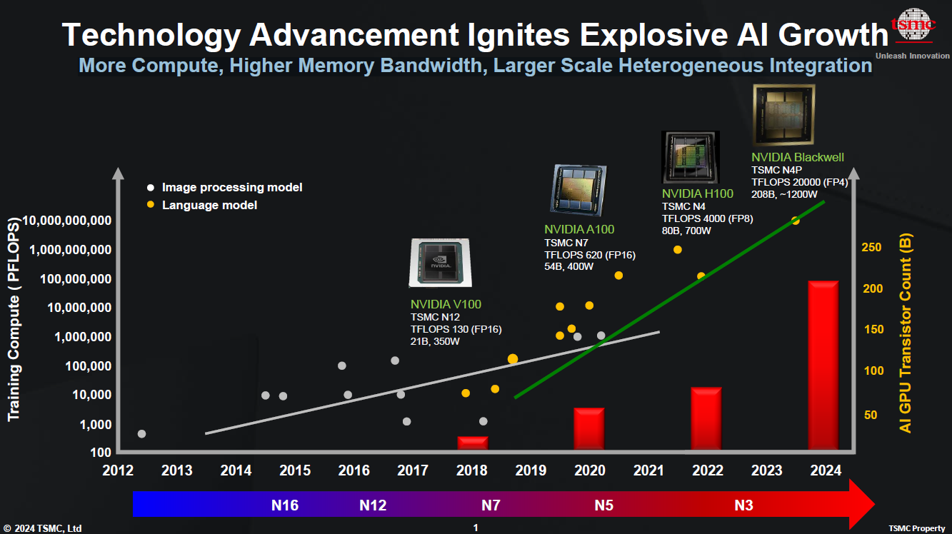 Source: TSMC
Figure 2
Source: TSMC
Dr. Hsiao-Chiang Chang began his presentation with a market-driven and TSMC's technology layout and brought out the following technology features, which are divided into two major parts: advanced process technology and advanced packaging technology, and are summarized as follows.
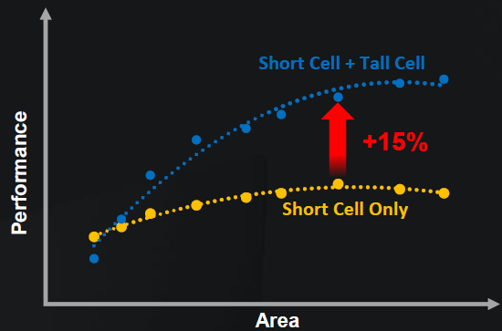
- NanoFlex technology innovation maximizes the value of nanochip transistors. The combination of Short Std. Cell + Tall Std. Cell maximizes the freedom of device width to obtain the best performance power area (PPA), which is 15% more than that of only Short Std. Cell, as shown in Fig. 3.
Figure 3
Source: TSMC
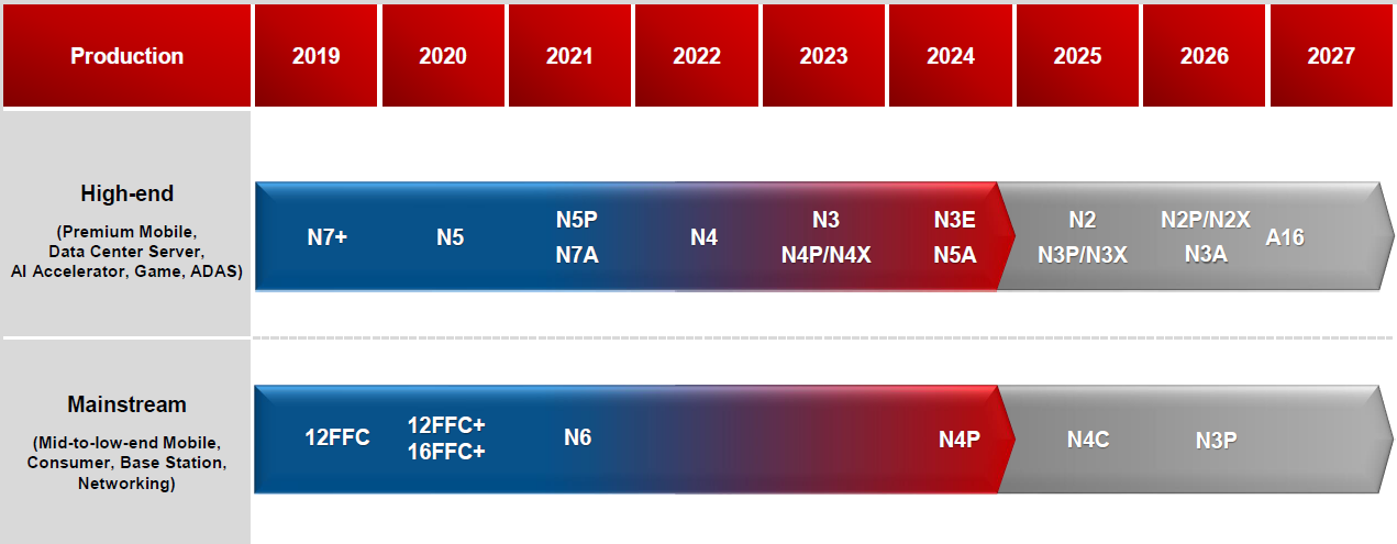
- A16 (1.6nm) will use Nanosheet process and is expected to be mass-produced in 2026, and for the first time adopts Super Power Rail (SPR), which will increase speed by 8~10%, save power consumption by 15~20%, and increase density by 1x compared to N2P.
- N4C is the most cost-effective 4nm process and is expected to be in volume production in 2025. The Cost reduction version of N4P saves 5% cost efficiency and the IP is fully compatible with N4P, which is a sweet balance between cost and performance.
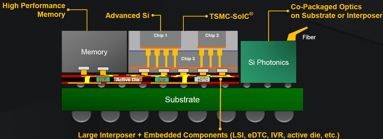
In the past, TSMC has released 3D Fabic, a platform that integrates 3D/2.5D packaging with SoIC integration, as mentioned in the previous Advanced Packaging Special Report.Analysis of Advanced Packaging Technology in High Performance Computing Chips (Next)The company will continue to develop new technologies to meet the needs of high-performance computing and artificial intelligence platforms in the future.] The future demand for high-performance computing and artificial intelligence platforms requires more advanced packaging (3D/2.5D), chiplet, and co-packing optics for vertical stacking packaging technologies, as shown in Figure 4. First of all, the processor part (Advanced Si in the picture) uses SoIC or 3D stack; high-performance memory (left side in the picture) uses high-bandwidth memory (HBM), and utilizes the intermediate lead redistribution layer and silicon intermediary board (Interposer) to connect the processor with the memory, which is the well-known CoWoS or InFO, which for impedance matching must also include embedded capacitive eDTC. For impedance matching, embedded capacitor eDTC and voltage regulator IVR circuits are included. For data transmission, co-packaged optics will be used to package the optical engine (optical/telecommunication signal converter silicon photonics) from the traditional PCB printed circuit board onto an ABF carrier board, which is closer to the processor and the storage chip. In other words, future high-performance computing and artificial intelligence platforms will utilize a large number of vertical stacking packages to integrate electrical and optical components.
Figure 4
Source: TSMC
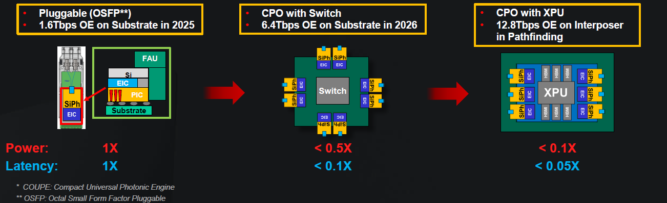
- COUPE (Compact Universal Photonic Engine) compact universal photonic engine using SoIC-X+3D packaging technology will be available in 2025, and in 2026 the electronics and photonics will be co-packaged in CoWoS, providing the ultimate in interconnect density with optimal power consumption. COUPE reduces power consumption by 2x and latency by 10x. Delay, as shown in Figure 5, left; packaged on a CoWoS silicon intermediate board, blue in Figure 5. COUPE reduces power consumption by a factor of 5 and latency by a factor of 2, as shown on the far right in Figure 5 below. [Previously in our introduction to COUPE:An Overview of the Development of Taiwan's Co-packaged Optical Industry]
Figure 5
Source: TSMC
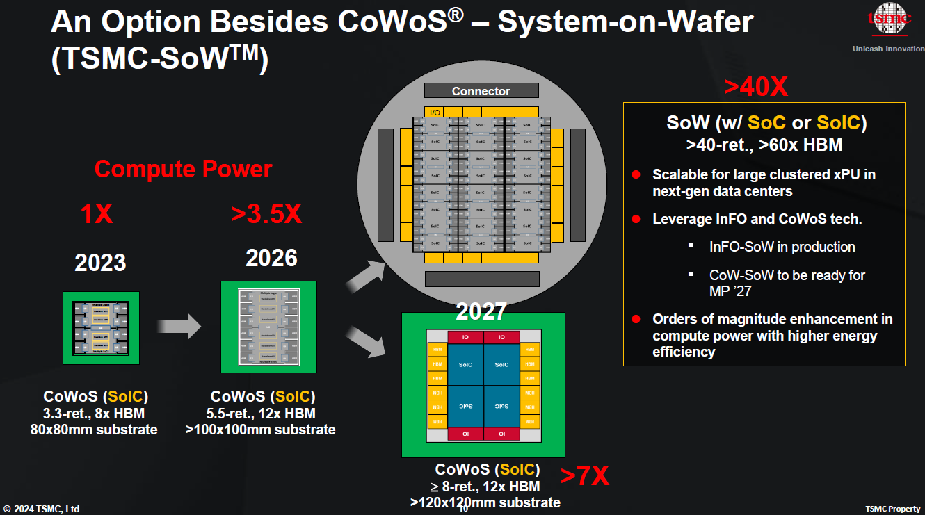
- The next generation of high-performance computing platforms in addition to CoWoS packaging, another option, SoW (System-on-Wafer) integrated 3D packaging + system-level wafers, directly on the whole wafer system, as shown in Figure 6 below. Taking 2023 CoWoS package as the starting point, using silicon intermediate boards is about 3 times the size of the photomask and can carry 8 HBMs; it is expected that by 2027 CoWoS package can be more than 8 times the size of the photomask and carry 12 HBMs, and if there is a need for larger package technology, SoW can be used, which is more than 40 times the size of the photomask, i.e., more than 40 times of computing power and more than 60 cells of HBM. This is suitable for next-generation large-scale data centers, the most famous of which is the Dojo chip for Tesla's supercomputer.
Figure 6
Source: TSMC
- The last automotive advanced packaging technology Automotive Advance Package InFO-os 5-layer RDL stacked carrier board technology, CoWoS-R 6-layer RDL lead redistribution technology, the target 2025Q4 through the automotive certification AEC Q100 Grade2, such as Figure 7.
Figure 7
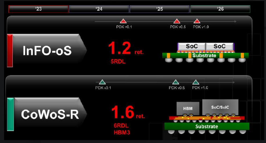
Source: TSMC
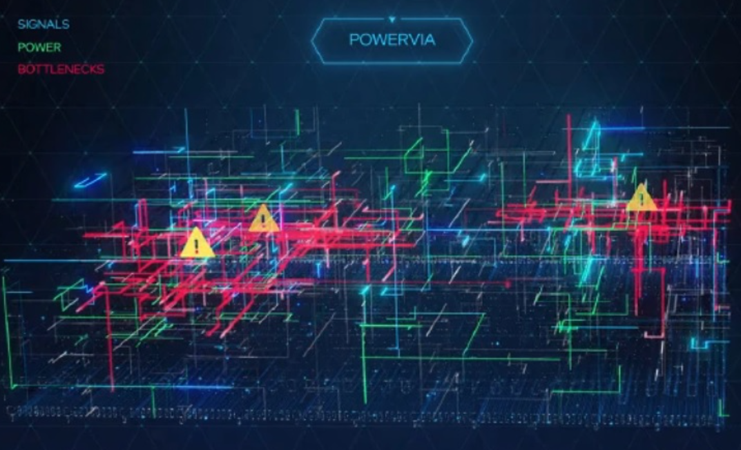
Continuing on from the above, the A16 (1.6nm) node will utilize a Nanosheet process and for the first time, a Super Power Rail (SPR). Super Power Rail (SPR) is an innovative backside power solution. The traditional power rail draws thicker wires for signal transmission on the M0 layer of BEOL in wafer manufacturing, and connects to the source/drain through the V0 layer and the MD layer of MEOL. However, as transistors get smaller and denser, the coexistence of signaling and power lines makes the circuit layer more and more complex and even chaotic, leading to signal interference, degradation of power consumption increases and other problems. Figure 8 below shows the signal simulation schematic provided by Intel, with the signal lines in blue, the power lines in green, and the areas of mutual interference and conflict in red, which shows that this problem is becoming more and more serious and cannot be ignored under the shrinking transistor.
Figure 8
Source: Intel
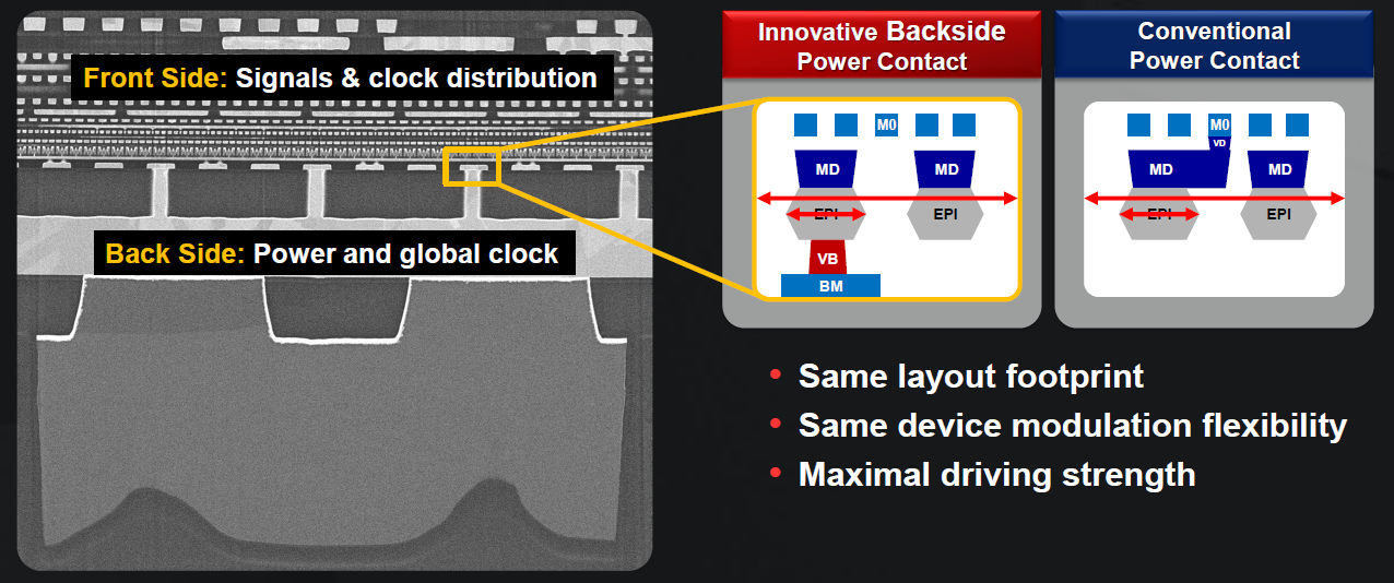
In addition, since the power rail requires thicker wires, which may occupy an area as high as 10%~20%, under the design of AI-driven extremely high-density transistors, the power rail has become a necessary evil to limit the increase of circuit complexity. Therefore, moving the power rail to the backside of the crystal and supplying power from the backside of the crystal allows the power lead not to shrink with the transistor, reduces the IR Drop effect, and maximizes the drive power strength under the same transistor layout, while maintaining the gate density and flexibility of component tuning; and allows the front side of the line to be dedicated to signal transmission, which improves the logic density and performance. The process TEM and schematic are shown in Figure 9 below.
Figure 9
Source: TSMC
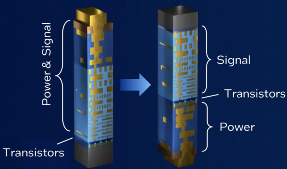
The same technology, competitor Intel in 2023 VLSI seminar has also proposed, which is called power column PowerVia technology, is expected in the second half of 2024 Intel 20A node into mass production. A report pointed out that Intel will Intel 20A process and Qualcomm (Qualcomm) production processor, but by the process of designing the chip input cost is too high, so Qualcomm decided to terminate the development, to maintain the original cooperation with TSMC, Samsung. However, it is not known whether the high cost came from switching suppliers or using Intel's PowerVia. The main process steps of the crystal back power supply should be similar in each supplier, first of all, or the front side of the transistor and connecting wires after the completion of the production (including the RDL layer), and then turn the wafer and grinding, revealing the bottom layer connected to the power cord. Most of the backside thickness is removed, from about 600 microns (um) to 300~100 nm, leaving a direct path for PowerVia's backside power supply, as shown in Figure 10, which is originally measured in microns. This process has certain difficulties and challenges to overcome relative to front-side power supply, including problems associated with substrate thinning, micron or nano silicon perforation (TSV) processes, wafer backside and front-side alignment, and the impact of the backside process on the front-end process actuator. Correspondingly, additional business opportunities such as milling machine upgrades, a huge increase in demand for milling consumables, and alignment machine upgrades are worth exploring in depth.
Figure 10
Source: Intel
Coincidentally, Samsung Semiconductor, another company with advanced process capability, is also offering the same technology, which is expected to be introduced in its own 1.4nm process node in 2027. A comparison of the backside power supply technologies of the three major advanced process providers is shown below, with no one having a clear advantage at this point in time, except for mass production.
Table 1
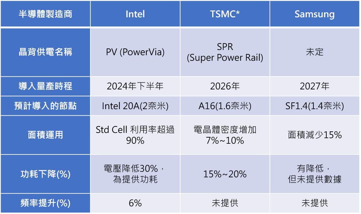
Source: TSMC, Intel, Korean media, compiled by Ji-Pu Industrial Trend Research Institute.
*TSMC data is a comparison with N2P (also using Nanosheet process, but not SPR), so the increase may be due to transistor shrinkage in the front end.
Summarizing these six highlights, we believe that advanced packaging platforms and CoWoS are driven by the demand of the largest number of end customers, just like the previous iPhone-driven InFo technology, even though the cost is high and the number of customers using it is small, it allows TSMC to continue to promote its technology to another level, and this development will enable TSMC to become less and less competitive in the advanced packaging field; in the case of the co-packaging optical CPO COUPE technology, since the specifications have not yet been determined, it is still necessary to see the final success of the cooperation partner's market share theory. In the joint packaging of optical CPO COUPE technology, since the specifications have not yet been determined, it is still necessary to look at the market share of the cooperation target to discuss the final success or failure, of course, do not rule out the major terminal chip vendors such as Broadcom and TSMC cooperation in the development of the relevant process, so that TSMC will continue to be the market leader in manufacturing; and NanoFlex technology and the most cost-effective mass production of the 4-nanometer process N4C, the two features can be a great deal to shine depending on the As the market leader, TSMC's core competencies of the fastest ramp up capability and the shortest learning curve are sure to be win-win tools to help customers and generate revenue. Last but not least is the crystal back-end supply technology, which will be an important technology introduction to open up or close the competition gap in the advanced process GAA (Gate All Around) competition. All three major vendors have put this technology into their product paths, and it seems that Intel will be the first to introduce it, but which one will be the last to introduce it in large quantities will depend on the necessity of the design, and the balance between cost and performance.
 April_Equipment|Taiwan Semiconductor Equipment Growth Strategy
 May_Sora|Visual Generative AI Technology and Application Development Overview(Up)