先進封裝設備材料專題|先進封裝CoWos台灣供應鏈發展概況
In the past few years, the trend of AI has made 2.5D/3D packaging become the most popular fried chicken, with the development of AI and large language model LLM (large language model), although the speed of pre-training Pre Training has slowed down the phenomenon, but Reinforcement Learning (Reinforcement learning) progress and expansion is about to begin; in addition, the launch of DeepSeek R1 model this Chinese New Year shocked Wall Street for a few days, they did come up with innovative model optimization and calculator configuration optimization, which is an innovative model optimization and calculator configuration optimization, which is a good idea for the development of AI. Expansion is just about to begin; in addition, in this year's Chinese New Year launched the DeepSeek R1 model shocked Wall Street for a few days, they did put forward an innovative model optimization and optimization of the calculator configuration, which is likely to make the ecosystem a little bit of a change. However, at a time when AGI, the general-purpose AI model, is not yet available, we don't think that DeepSeek's emergence will bring down the demand for ICs, but will instead bring up the demand for ICs (not only GPUs, but also CPUs, NPUs, ASICs, FPGAs, etc.), which will continue to push up the demand for advanced packages. From the end of 2024 to February 2025, the entire market demand for TSMC's CoWoS for the whole year will remain hot even in 2026, which shows that the current market still prefers to err on the side of letting go.
Among 2.5D ICs, the most representative is TSMC's CoWoS technology. It was in 2009 that TSMC's then Senior Vice President of Research and Development, Mr. Shang-Yi Chiang, and his R&D staff discovered that advanced packaging could make up for the loss of speed in data transmission on the chip. At the time of the launch of this technology, due to the complexity of the equipment used in this technology, the price is not compared to the advanced manufacturing process, so for foreign investors in the international community is like "killing the chicken with a bull's-eye," coupled with the fact that at that time, no one could see the commercial potential of CoWoS, many foreign companies are reluctant to cooperate with the provision of equipment, which in turn, Taiwan's equipment vendors to open up a path of opportunity. CoWoS technology can be divided into "CoW" and "WoS", as shown in Fig. 1 and Fig. 2 (organized for CoWoS-S), and its overall process relies on a variety of equipment, such as crystal picking equipment and dispensers,
- 揀晶設備:主要是挑揀出通過檢測的晶片,並將合格的晶片排列在中介層上,在透過固晶設備以微凸塊(uBump)進行黏晶,使晶片固定在Si interposer。其中揀晶設備及黏晶機皆為均華提供。
- 點膠機:封裝過程中會需要點膠設備用來協助晶片點膠,以此實現晶片堆疊。主要供應商為萬潤。
- 化學清洗:為半導體製造的關鍵步驟,用於去除晶片上的汙染源,而汙染源主要分為五種,分別為微粒子、金屬不純物、有機物、表面微粗糙度、自然生成氧化層。每個汙染源可能對晶片造成的影響也有所不同。主要供應商是弘塑、辛耘。
- 晶片鍵合:過去5D、3D封裝都是採用Solder Bump(銲錫凸塊/焊球)或Micro Bump(微型凸塊)來實現晶片與基板、中介層的連接,而在該技術上所有植球的步驟都是使用錫球。不過當Bump pitch(凸塊間距)小於10~20nm時,錫球的鍵合就成為了製程的難點,因此Hybrid Bonding在高運算需求的時代橫空出世。其晶片連接的技術是通過金屬(如銅)和氧化物鍵合,可降低凸塊的間距、提升連接密度,達到更快的傳輸速度並且降低能耗。主要供應商為荷蘭貝斯半導體(Besi)為較高精度機台,日本的芝浦先進(Shibaura)持續改善技術獲取市佔。
- 濕式蝕刻:是指使用化學液去除表面特定區域的材料,優點在於製程簡單、成本低、蝕刻選擇多且產量速度較快。主要供應商為弘塑。
- 自動光學檢測(AOI):自動光學檢查是運用機器視覺做為檢測技術,以改進或彌補人力光學檢測的缺陷。AOI的主要功能包括瑕疵檢測、尺寸測量和定位貼合。目前在CoW端的AOI相關檢測部分,依舊是外商的天下,台商要進駐還需時間,因此台廠多瞄準後段oS檢測市場,而CoWoS供應鏈中,均豪不只提供AOI光學檢測設備,還供應可以驗證AOI光學檢測設備準確性的白光干涉量測設備;另牧德也與家登開發AOI自動光學檢查系統,結合科嶠的載具清洗機,將成為CoWoS全方位載具多功能清洗檢查機。
圖一、CoWoS中的CoW製造流程
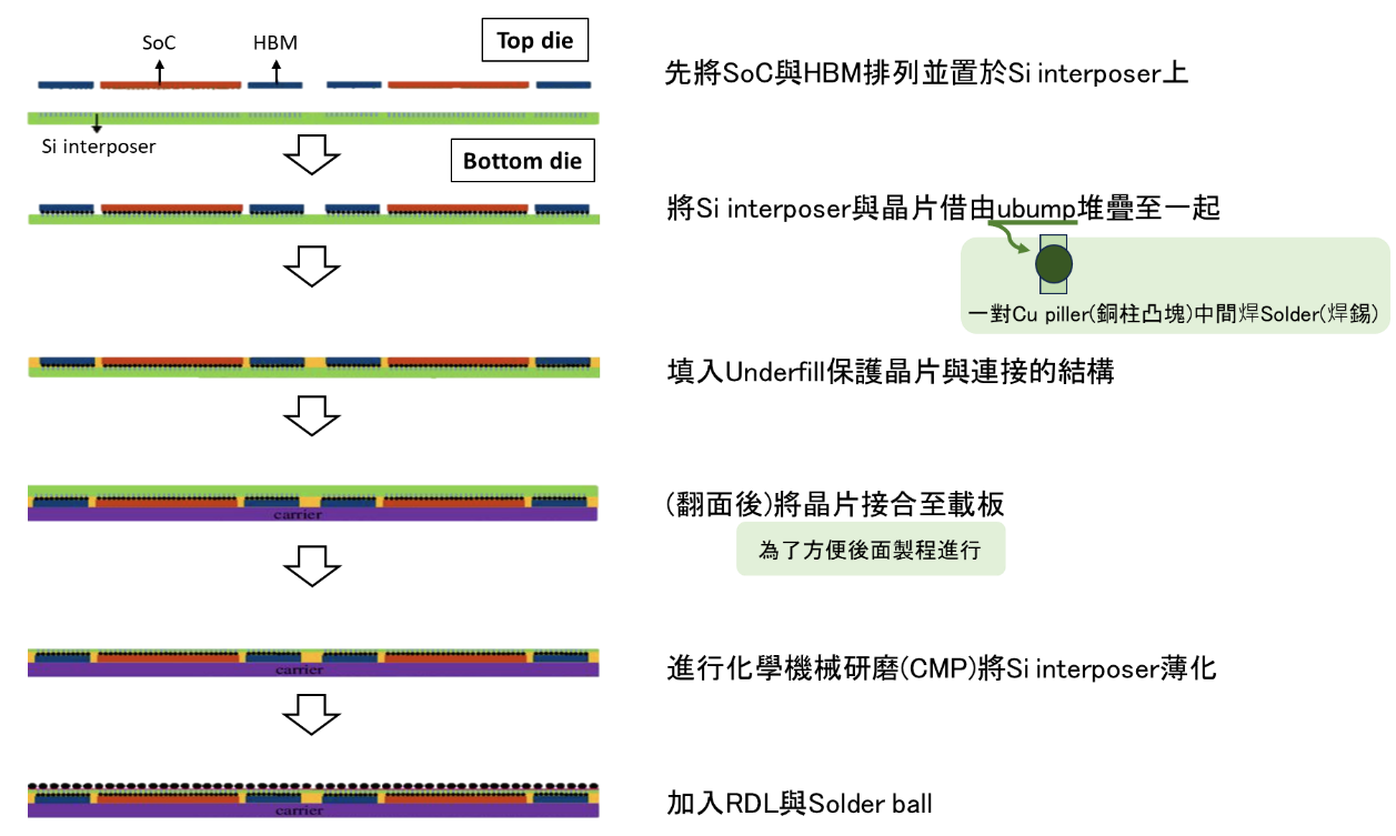
Source: Ji-Pu Industrial Trend Research Institute
圖二、CoWoS中的WoS製造流程
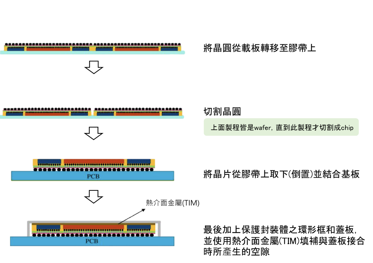
Source: Ji-Pu Industrial Trend Research Institute
另外,CoWoS的重要製程材料有矽中介層、PCB基板、化學品、測試板卡等,說明如下:
- 矽中介層:CoWoS通過運算邏輯晶片和HBM晶片安裝在矽中介層上,再直接放置在封裝基板上以整合邏輯運算和HBM晶片。除了高密度連接之外,矽中介層在緩解封裝基板(樹脂基板)和矽晶片(邏輯晶片、存儲器晶片等)之間發生的熱變形方面也扮演著重要的角色(因熱失真會導致電路操作延遲)。而目前聯電成功打進CoWoS矽中介層的供應行列,並進入量產階段。
- PCB基板:在CoWoS製程中,PCB基板提供機械支撐、訊號傳輸、熱管理與散熱功能,並整合電源與接地層。它連接多晶片模組,提升可靠性,確保高效能封裝的穩定性與製程整合,為晶片堆疊與應用奠定關鍵基礎。而提供PCB基板的供應商為楠梓電,另外於供應鏈中提供IC載板(ABF)的為欣興。
- 化學品:化學品在CoWoS製程中負責清潔、蝕刻、光刻、電鍍及黏著,確保表面潔淨、結構精密及導電路徑形成,並提供穩定性與保護。不同化學品的特性,會導致在設備內的流體狀態不同。弘塑2013年併購化學品供應商添鴻科技,除了在設備銷售外,還多了一個持續創造營收的耗材事業。弘塑在機台設備營收占比約為四成以上,而半導體相關製程用化學品約占兩成多。
- 測試板卡:負責功能驗證、性能測試、可靠性檢測、製程優化與系統整合,確保封裝品質與效能(主要用於封裝後的測試階段,如CoWoS;通常是一塊多層PCB板,包含測試電路、接頭和控制接口,用來檢驗完整的模組),並提升製程良率與產品穩定性。主要供應商為精測。
CoWoS 技術的蓬勃發展不僅帶動了半導體產業的革新,也為市場注入一股新的活力。隨著 CoWoS 技術的發展,相關台灣設備供應商也備受關注。許多本土設備商如辛耘、弘塑、均華、志聖、萬潤、欣興、家登等,正因為CoWoS乘風崛起(如圖三)。從過去僅是晶圓代工廠的「備選」、採購順位總排在外商之後的B咖,變成A咖。這是第一次由台灣本土設備業者,從無到有,定義產業規範,是台灣史上首次擁有這麼完整的科技話語權。
圖三、CoWoS台灣供應商概述
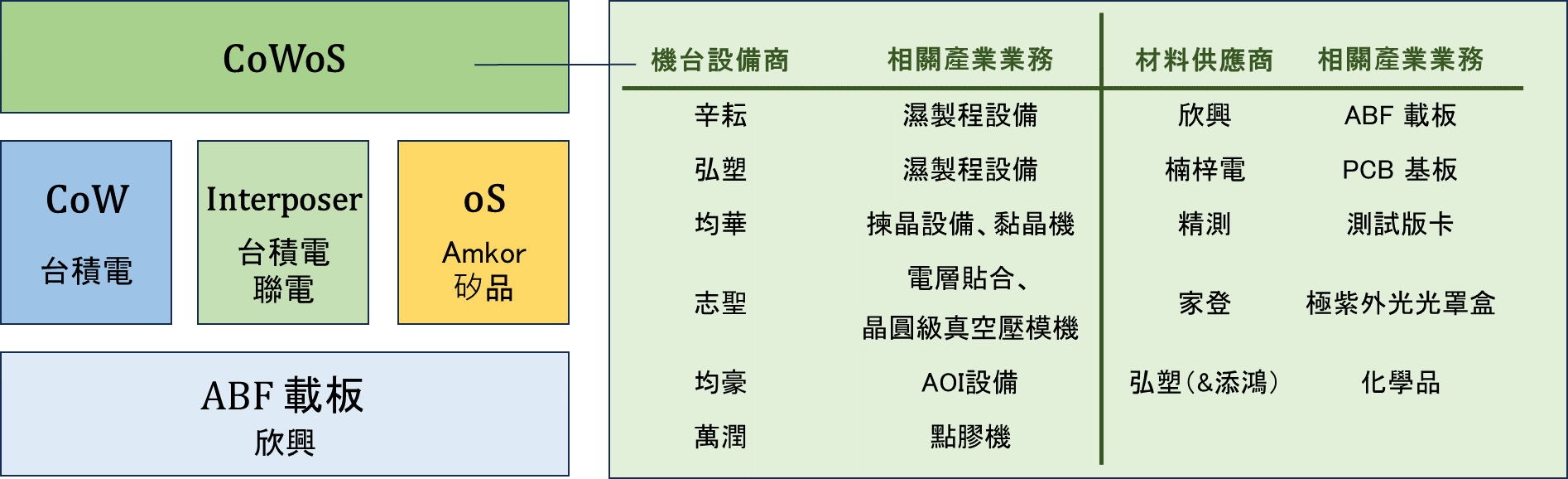
Source: Ji-Pu Industrial Trend Research Institute
最後,隨着AI高算晶片的發展,CoWoS封裝技術不僅是半導體產業的革新引擎,更是驅動2.5D/3D晶片整合浪潮的關鍵力量。隨著技術的不斷演進和應用場景的拓展,CoWoS將在未來持續引領半導體產業的創新與發展,為投資者帶來無限的想像空間。掌握CoWoS技術的發展趨勢,將是投資者洞悉未來科技浪潮的關鍵。呼應先前文章《美中科技戰所牽動之半導體產業脈動》and《2.5D/3D封裝之重要性與關鍵的製程點》,在後默爾定律下,先進封裝技術對半導體產業的深遠影響,加上川普上任後,美國限制中國AI晶片發展不減反增以及川普持續釋放對台灣半導體不友善的言論來看。目前不只先進封裝的關鍵設備材料禁止輸中,像是混和鍵合(Hybrid bonding)、晶圓薄化(Wafer Thinning)、模封材料LMC等很有機會,台灣廠商與供應鏈到美國設立相關先進封裝製造據點也非常有可能,以上產業脈動與商機值得我們持續的注意觀察。