面板級封裝專題|扇出型面板級封裝(FOPLP)市場與技術發展概況
According to a report released by market research firm Yole Développement, the global fan-out packaging market will reach US$1.86 billion in 2022 and is expected to grow to US$3.43 billion in 2026, with major applications such as mobile devices and consumer electronics, telecommunications and infrastructure, and automotive accounting for US$1.61, US$1.60, and US$0.22 billion, respectively, and wafer foundries, The market shares of outsourced packaging and testing foundries and integrated component manufacturers are 71%, 19% and 10% respectively, while the market shares of fan-out wafer-level and panel-level packages are 87% and 13% respectively. UHD FOs with more than 18 I/Os per square millimeter and line width/spacing of the rewire layer of less than 5μm, HD FOs with I/Os per square millimeter between 6 and 12 and line width/spacing of the rewire layer of between 5μm and 15μm, and Core FOs with I/Os per square millimeter less than 6 and line width/spacing of the rewire layer of 15μm or greater, which are expected to be available by 2026.
Currently, fan-out wafer-level packaging uses high-precision process equipment, with redistributed line layers often exceeding 5 layers and line width/spacing less than 5 μm, and is mainly used for packaging of chips with a higher density of I/O contacts, such as central processors, graphic processors, application processors, special application integrated circuits, field-programmable logic gate arrays, and radio frequency. Fan-out panel-level packages use relatively low-precision process equipment, generally with less than four layers of rewiring and a line width/spacing of more than 5μm, and are mainly used for packaging I/O chips with a lower density of contacts, such as power management, microelectromechanics, sensors, and so on. According to a report released by market research firm Yole Développement, the global fan-out panel-level packaging market will reach US$41 million in 2022, and is expected to grow to US$221 million by 2028, with an average annual compound growth rate of 32.5%, which is significantly better than the overall fan-out packaging market of 12.5%, due to a low base period. By 2028, the annual production volume of fan-out wafer-level packaging will reach 2.376 million 12-inch wafer-equivalent, while the production area of fan-out panel-level packaging will be 238,000 12-inch wafer-equivalent, which is only one-tenth of that of the former, indicating that the market scale is limited to expand. Although fan-out panel level packaging has been developed for a long time, there are still a lot of problems encountered in the development process, including: less mature and more expensive equipment and materials, lower process yields, and large warpage problems to be overcome. The problem of non-standardization of substrate size that existed at the early stage of development has been solved. In 2019, the International Semiconductor Industry Association (ISIA) formulated SEMI 3D20-0719 specification, which limits the use of substrates for fan-out panel-level packaging to two sizes, namely, 510mm x 515mm and 600mm x 600mm.
Inheriting the fan-out wafer level packaging technology, the current fan-out panel level packaging still adopts two kinds of processes, such as Chip First and RDL First, etc. The earliest development of fan-out wafer level packaging technology, such as Infineon's eWLB and Freescale Semiconductor's RCP, use Chip First process, which can be subdivided into two kinds of processes, such as Face Down and Face Up, etc. The process flow is shown in Figure 1. It can be further divided into two categories, such as Face Down and Face Up, and its process flow is shown in Figure 1.
Left) Face Down sequence: (1). Wafer dicing; (2). The wafer is bonded to a temporary substrate coated with a pyrolytic film with the I/O contacts facing down; (3). Fill the wafer with mold sealing material and then heat cure; (4). Heat to release the sealed wafer from the temporary substrate, and then make the rewiring layer and implant the solder balls on the I/O contact surface; (5). Dicing into a single component.
(Right) Face Up sequence is (1). Wafer dicing; (2). The wafer is bonded to a temporary substrate coated with a pyrolytic film with the I/O contacts facing down; (3). Fill the die with mold sealing material and heat cure; (4). Thinning the seal to expose the I/O contacts of the wafer, then making the rewiring layer and implanting the solder balls; (5). Heat the molded die to release the temporary substrate; (6). Dicing into a single component.
Figure 1: Chip First's Face Down (left) and Face Up (right) process flow diagrams
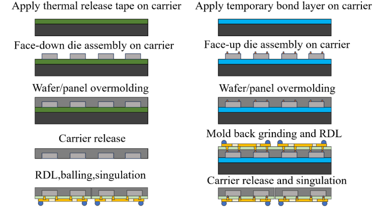
Source : IEEE
The main drawbacks of the Chip First process include:
(1). The curing temperature of the molding material should not be too high, otherwise it will damage the chip, but using low curing temperature molding material will not provide sufficient protection due to poor mechanical properties;
(2). The I/O contact spacing of the chip is limited by the process accuracy of the rewiring layer;
(3). The production of rewiring layer requires high precision of wafer position, and the slightest substrate warpage will cause the wafer to shift, which will easily lead to process defects;
(4). Wafers adhered to the defective areas of the process in the rewiring layer will be scrapped, so it is not easy to maintain a high yield rate.
To address these shortcomings, Deca Technologies, a subsidiary of Cypress Semiconductor, proposed RDL First technology in 2012, whose process flow is shown in Figure 2, in order:
(1). Create a rewire layer on a temporary substrate coated with a pyrolytic film to prevent the substrate from warping and affecting its process yield;
(2). Attach the chip to the rewiring layer with the I/O contacts facing down;
(3). Mold-sealed wafers;
(4). Heat the wafer to detach the temporary substrate and implant the solder balls;
(5). Dicing into a single die assembly. The advantage of this technology is that the characteristics of the rewired layers can be detected in advance, avoiding the need to paste the wafers in the defective areas of the process to increase the yield rate and reduce the wasted production cost and time.
Figure 2: RDL First Process Flow Diagram
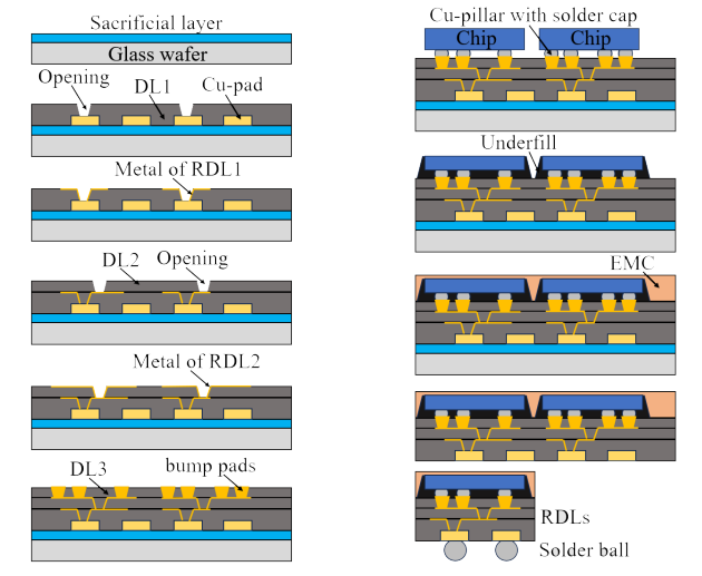
Source : IEEE
A comparison of Chip First and RDL First processes for fan-out panel level packaging by market research firm Yole Développement is shown in Table 1, which shows that the performance of both processes is consistent in terms of component integration and physical characteristics.butRDL FirstBetter electrical characteristics(math.) genusThese include larger bandwidths, the ability to provide moreI/OGood contact number and shielding performanceSubstrate warpage and wafer displacement are the main problems encountered in fan-out wafer level packaging processes. Substrate warpage and wafer displacement are the main problems encountered in fan-out wafer level packaging processes. The solution for the former is to perform stress simulation analysis to select the appropriate substrate or dielectric layer material, while the solution for the latter is to compensate for the offset during exposure or to use wafer adhesives to reduce the amount of offset caused by high temperatures.
Table 1: Comparison of Chip First and RDL Frist Processes for Fan-out Wafer Level Packaging
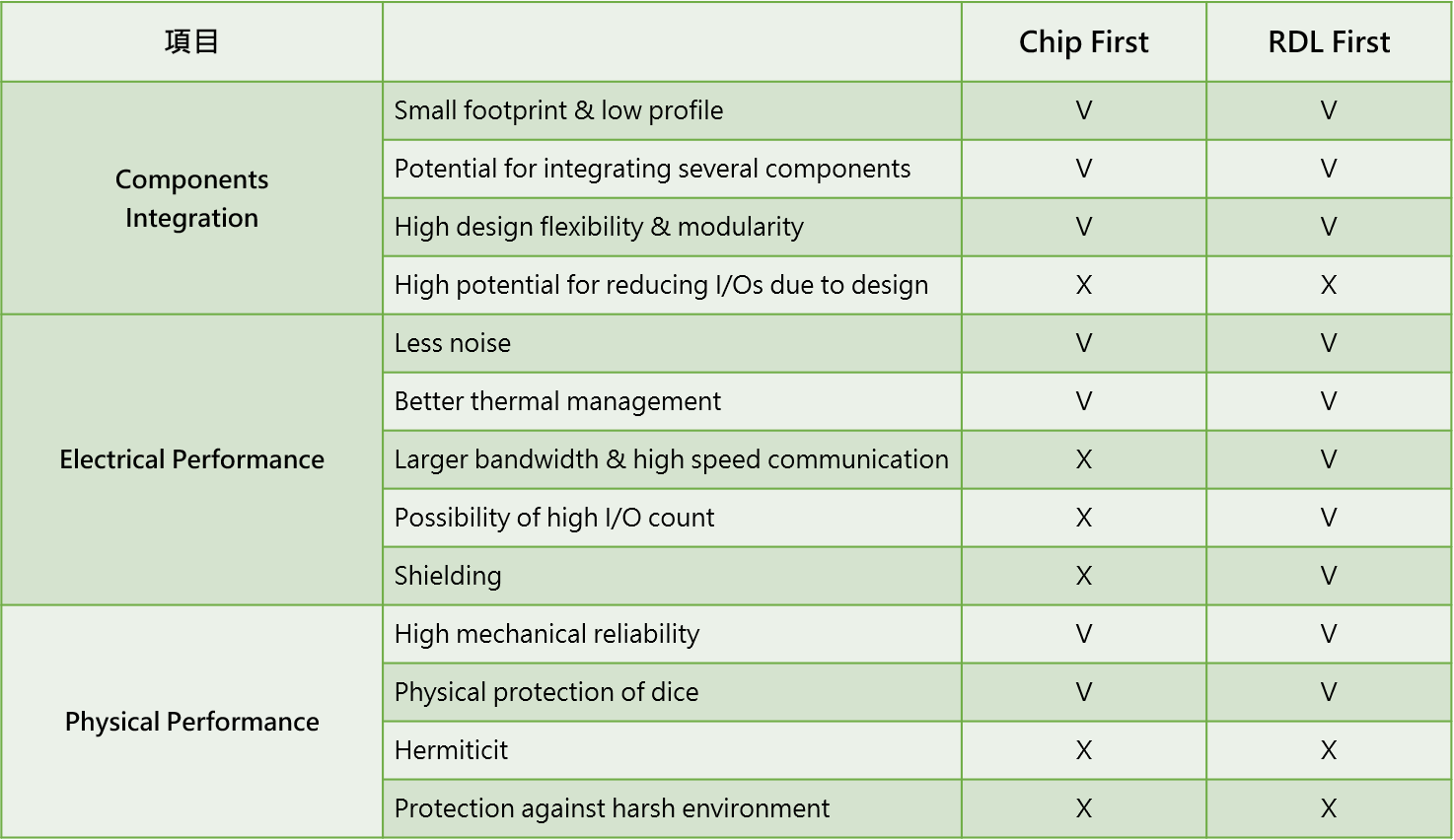
Source : Yole Développement; Collated by Ji-Pu Industrial Trend Research Institute, 2024/09
In addition, the temporary substrates used in the fan-out panel level packaging process are mainly stainless steel or glass. Due to its excellent dimensional stability, surface flatness, and thermal conductivity, semiconductor manufacturers have been studying the application of glass in 2.5D/3D packaging substrates or intermediate layers, for which through glass vias (TGVs) need to be made for signal connections between the packaging components and the motherboard. For this purpose, Through Glass Via (TGV) needs to be made for the signal connection between the package and the motherboard. Compared with the Through-Silicon Via (TSV) drilling and filling of holes are used in the semiconductor process of etching and plating machine, TGV drilling and filling of holes in the two parts of the drilling and filling of holes so far has been developed micro-abrasive, electrical discharge machining, ultrasonic drilling, laser drilling, plasma etching, Laser Induced Deep Etching (LIDE) and other drilling technologies to Laser Induced Deep Etching (LIDE), which is the most effective way of drilling and filling holes in the TGV. Deep Etching (LIDE) has more advantages in mass production. It utilizes pulsed laser for directional modification of the glass substrate, and the etching rate of the irradiated area in hydrofluoric acid is faster than that of the unmodified area, so it can be wet-etched to form through-holes. LPKF of Germany was the first to introduce laser-induced etching equipment for glass through-holes, and its advantages include: (1). Uniform hole formation quality without cracks and thermal stress residue; (2). Fast through-hole formation, up to 5000 through-holes per second; (3). Realize high-precision microvias with diameters as low as 10 μm and depth-to-width ratios as high as 10:1; (4). Laser parameters can be adjusted to control through-hole perpendicularity and hole wall morphology; (5). Reduced production costs by eliminating the need for micrographic process equipment and photomasks.
Filling holes is mainly done by sputtering to deposit seed layer on the hole wall and then electroplating copper to achieve seamless filling, nowadays, three plating methods have been developed such as Bottom-Up, Butterfly Mode, and Conformal, etc. Bottom-Up is used for blind holes with no connection at the top and bottom, which utilizes additives to accelerate the bottom but inhibit the deposition speed of the sidewalls, so that copper plating direction moves up from the bottom to the top. Butterfly Mode is the plating mode for vertical side-wall through-hole, which prioritizes deposition of the center and then moves the plating direction up and down, while Conformal is the plating mode for circular and inclined side-wall through-hole, which allows the center and side-walls to deposit at the same rate in order to avoid creating holes.