面板級封裝專題|全球扇出型面板級封裝(FOPLP)發展狀況
隨著半導體前段先進製程已逼近物理極限,倚靠縮小元件尺寸以提高其運行能力勢必面臨生產成本節節高漲的問題,於是全球半導體業界將先進封裝視為延續摩爾定律生命週期的關鍵技術,實現以較低成本生產更高性能、更低耗電量、訊號傳輸速度更快的晶片。在2024 年進入下半年,面板級扇出型封裝(FOPLP)成為備受關注的下一代先進封裝技術,除了台積電在法說會提到之外,Semicon Taiwan 2024 國際半導體展中,也將面板級扇出型封裝(FOPLP)列為焦點,同時也是封測廠、面板廠極力佈局的方向。
Traditional semiconductor packaging is a technology that cuts wafers into chips and then packages them individually. The wafers are connected to the lead frame or substrate through peripheral wire bonding, and as the number of I/O contacts continues to increase, the wire bonding is not enough, which is why it gradually entered the market in the 1990s.
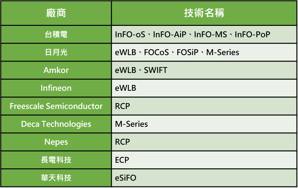
In 2006, Infineon was the first to develop fan-out wafer-level packaging technology for cellular baseband chips, called Embedded Wafer Level Ball Grid Array (eWLB). At the same time, Freescale Semiconductor also proposed Redistributed Chip Packaging (RCP) technology for radar and Internet of Things (IoT) chips. The number of I/O contacts of these two fan-out wafer-level packaging pioneers is usually less than 500, and the line widths and spacings of the redistributed line layers are also larger. The performance improvement is limited, so it has not been emphasized by the industry. At this time, with the introduction of high sensitivity photoresist and high resolution exposure machine, fan-in wafer level packaging technology has been developed rapidly, making the higher cost of fan-out wafer level packaging to face its fierce competition and fall into a development bottleneck, such as Intel abandoned the use of the technology to package cell phone baseband chips until 2016 to show the light of day. After nearly a decade of research and development, TSMC launched the Integrated Fan-Out (InFO) packaging technology, which was successfully applied to the A10 application processor of Apple's iPhone 7 series cell phone, with a high price/performance ratio that made it continue to be used in subsequent iPhone APs. The advantage of the integrated fan-out packaging technology is that it eliminates the need for substrates and reduces the cost by more than 20%~30% compared with the traditional Package on Package (PoP) technology, and it can be applied to different types of wafers, for example, the 8mm x 8mm platform is suitable for the packaging of radio-frequency and wireless wafers, the 15mm x 15mm platform is suitable for the packaging of application processors and baseband wafers, and the 25mm x 25mm platform is suitable for the packaging of application processors and baseband wafers. For example, the 8mm x 8mm platform is suitable for RF and wireless chip packaging, the 15mm x 15mm platform is suitable for application processor and baseband chip packaging, and the 25mm x 25mm platform is suitable for graphics processor and communication chip packaging. So far, major chip makers and packaging foundries have laid out fan-out wafer-level packaging technology, the index vendor technology as listed in Table 1. Among them, TSMC and Sun Micron have also launched their own fan-out wafer-level packaging technologies for different applications. In TSMC's part, high-performance computing wafers are packaged with InFO-oS technology, server processor wafers and memories are packaged with InFO-MS technology, wireless communication wafers are packaged with InFO-AiP technology, and InFO-PoP has been introduced into the 3D packaging technology to allow random access memory (DRAM) stacks to be packaged. DRAM is stacked on top of the mobile application processor (AP); in the Sun Microsystems part, chips for baseband, RF, vehicle, radar, and decoding can be packaged in eWLB technology, while chips for network and server processors are mainly packaged in FOCoS technology, and chips for baseband, RF, power management, and decoding can be packaged in M-Series technology, while chips for RF, power, and microprocessor applications can be packaged in FOSiP technology. Chips for RF, power, and microprocessor applications can be packaged in FOSiP technology, of which M-Series is a technology transfer from Deca Technologies.
Table 1: Names of Fan-Out Wafer-Level Packaging (FOWLP) Technologies Developed by Key Vendors
Source : LightCounting; Collated by Ji-Pu Industrial Trend Research Institute, 2024/09
In recent years, with the rise of new applications such as artificial intelligence, intelligent driving, and humanoid robots driving huge demand for high-performance computing SoCs, TSMC's CoWoS packaging capacity has been in short supply, and so TSMC's development of fan-out panel level packaging technology has become the focus of the industry. Its main advantage is that it can reduce production costs due to its large single-chip throughput and high area utilization rate. The area utilization rate of fan-out wafer-level packaging is less than 85%, while that of fan-out panel-level packaging is more than 95%. Comparing a 600mm x 600mm fan-out panel-level packaging with a 12-inch (300mm) fan-out wafer-level packaging, the former has 5.7 times the wafer throughput of the latter, as estimated by market researcher Yole Développement. Market research firm Yole Développement estimated that the cost of the former is at least 20% lower than that of the latter, as shown in Figure 1.
Fig. 1: Cost comparison between fan-out wafer-level packaging and fan-out panel-level packaging
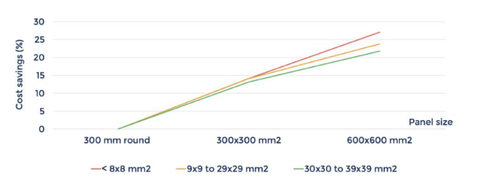
Source : Yole Développement
At ECTC2011, Japanese foundry J-Devices was the first to introduce Wide Strip Fan-out Package (WFOPTM) technology for packaging on 320mm x 320mm metal substrates, and was the first in the world to introduce a fan-out panel-level package that applies printed circuit board manufacturing process technology to create a redistributed layer of 20μm line width/space. At ECTC2012, Fraunhofer IZM, a German research institute, announced its fan-out panel level packaging technology for wafer packaging on 610 mm x 457 mm plastic substrates using Compression Molding, which employs dry-film photoresist and Laser Direct Imaging (LDI). It uses dry-film photoresist and laser direct imaging (LDI) equipment to produce the rewiring layer, and the size of the encapsulated device is 8mm x 8mm with two 2mm x 3mm wafers inside. The wafer is embedded in a dry film and is not a liquid mold sealing material, and there is only a single wiring layer. Subsequently, Sun Micron, Li-Cheng, EGAC, Semco, Nepes, Deca Technology, and other manufacturers introduced fan-out panel-level packaging technology into mass production, and the substrate sizes used are listed in Table 2, but Sun Micron, EGAC, and other major packaging and testing companies are still mainly producing fan-out wafer-level packaging, and the production volume of fan-out panel-level packaging is small.1 Semco is the current leader, which is a substrate manufacturer of the Samsung Group, and was launched in 2016. Semco is the current leading manufacturer, which is a substrate manufacturer of Samsung Group, invested 264 billion won in 2016 in Cheonan, Chungcheongnam-do, South Korea, to set up a fan-out panel-level packaging plant, which adopts a plastic substrate of 510mm x 415mm and will be mass-produced in 2018, and has tested large-size panels of 800mm x 600mm. At the beginning of mass production, it was used for Galaxy Watch processor packaging. In 2019, the production line was acquired by Samsung Electronics, and in 2023, the Tensor G2 processor of the Pixel 7 cell phone produced by its OEM will use the FOPLP-PoP technology that stacks DRAM on the application processor. In recent years, more and more industry players have been investing in the R&D of fan-out crystal panel packaging technology, which is roughly divided into four fields: foundry, packaging and testing foundry, carrier board, and LCD display manufacturers. Carrier boards and LCD display manufacturers with no experience in packaging and testing are often in need of technical cooperation.
TSMC Chairman and President Chieh-Chia Wei personally confirmed at the July 18th press conference that FOPLP (Fan-Out Packaging at Panel Level) is in full swing. It is reported that TSMC has set up a research and development team and production line, is still in the initial stage, Wei Zhejia forecast, 3 years time is expected to be able to have the relevant results. (Domestic and foreign equipment vendors, packaging and testing factories, panel makers all hot, together with the sprint technology landing). It is reported that the size of the rectangular substrate in the test is 510 × 515mm, but there is news that the new finalized version is 600 × 600mm.
Table 2: Substrate sizes used by fan-out panel level packaging vendors

Source : Yole Développement; Collated by Ji-Pu Industrial Trend Research Institute, 2024/09