
矽光子專題|全球矽光子市場概況分析(上)
With the rapid development of new technologies such as AI, IoT, and 5G driving the demand for huge amounts of data computation, in addition to the use of high-speed computing chips, inter-chip communication is another key factor to increase the speed of computation. However, the current copper wire transmission is unable to meet this demand due to the problems of signal loss and heat generation, so it is important to introduce optical signal communication. Since light waves carry no charge, have no static mass, do not interfere with each other within the same channel, and have low signal loss and heat generation, they are the best solution for transmitting huge amounts of data, which meets the three major requirements of long transmission distance, large bandwidth, and low energy consumption. Generally, optical communication modules for transmitting and receiving signals include optoelectronic components such as lasers, optical switches, modulators, detectors, etc., and optical components such as waveguides, couplers, filters, etc. In the past, these components were placed on circuit boards, but integrating them into a single chip can increase the speed of signal transmission and reduce energy consumption. Silicon photonics technology for wafer fabrication has been developed because silicon has the following advantages.
- 光通訊波長一般介於1310~1550 nm,矽不吸收此段波長光線而可避免損傷。
- 矽和二氧化矽的折射率對比大,有助於縮減元件尺寸以提高晶片的集成密度。
- 元件製作使用的SOI技術與矽晶片製程相容性高,可顯著降低生產成本。
圖1、矽光子晶片架構示意圖
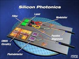
資料來源 : Intel (2023)
最早於1969年美國貝爾實驗室研究員S.E.Miller首次提出積體光學概念,1985年Richard Soref提出矽光子積體電路的構想,1993年再出示矽光子晶片結構示意圖,但直到2000年後因為半導體製程技術進入次微米時代才逐步實現,此時歐盟、日本、美國政府提供計畫經費支持矽光子技術發展,2004年起歐盟透過FP6計畫投資矽光子基礎科學研究,並由比利時IMEC與法國CEA-Leti合作成立ePIXfab聯盟以建構光通訊技術平台,2008年起藉由FP7計畫資金降低參與門檻以推展矽光子技術,2012年後該聯盟增加芬蘭VTT、荷蘭TNO、德國IHP Microelectronics、愛爾蘭Tyndall、加拿大CMC Microsystems等科研機構合作夥伴以提供各式矽光子技術服務,藉此扶植完整產業鏈;日本主要透過國家型光電整合系統技術(PECST)計畫支持矽光子技術發展,參與者包括東京大學、京都大學、東京技術學院、橫濱國立大學、產業技術綜合研究所、光電子融合基盤技術研究所等科研機構與Fujitsu、Furukawa Electric、NEC、NEL、NTT、OITDA、OKI、Toshiba等企業,主要任務是研發光子電路整合與封裝關鍵技術,以達到2025年開發出光電整合晶片之目標;2013 年美國成立國家光子計畫(NPI),2015年於New York州Rochester市建立美國積體光子製造組織(AIM Photonics),目前由New York州立大學科研基金會主導,成員包括Intel、IBM、GE、Infinera、HP、Acacia、GlobalFoundries等科技大廠,運作費用由聯邦基金與成員共同分擔以發展美國矽光子產業生態鏈。
政府計畫促成IBM、Intel、NTT、NEC、Sun Microsystems等參與企業設立矽光子部門並投入大量資源開發其元件與晶片技術,其中IBM和Intel還推出矽光子相關產品。2010年後矽光子技術進入高速發展時期,藉助風險投資陸續成立Luxtera、Kotura、Mellanox、Lightwire、Macom、Aurrion和Acacia等小型新創公司,部分被大企業併購後還持續投入資金已成為當前矽光子產業擴展方式。