異質整合專題|先進封裝之重要製程技術發展趨勢解析(下)
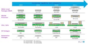
In recent years, the commercialization of applications such as the Internet of Things, big data, 5G communications, artificial intelligence, self-driving cars, and smart manufacturing has prompted semiconductor manufacturers to actively introduce advanced packaging technologies to meet customer demand for thinner and lighter wafers with faster data processing speeds and lower power losses. Therefore, the market mainly comes from computer and mobile device processors with complex functions and high-speed computation. As shown in Figure 2, the most powerful CPU/GPU will be the first to introduce the most advanced 2.5D/3D packaging technology in 2020, while the packaging technology used for mobile device processor ICs and RF ICs will lag behind by two or three generations respectively, and automotive ICs, which are simple in functionality but require higher weather resistance, will continue to utilize traditional packaging technology.
Figure 2: Changes in Semiconductor Packaging Technology for Different End Products
Source : KLA Tenco
圖3、先進封裝的關鍵技術發展藍圖
Source : Yole Développement
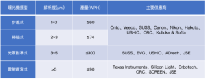
表4、四種曝光機的重要性能比較與主要供應商
Source : Yole Développement
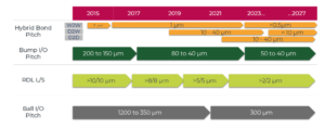
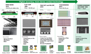
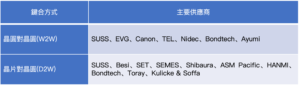
鍵合是將晶圓或晶片對準後連接以實現訊號相互導通,使用中間介質層與否分為直接與間接鍵合等兩類,先進封裝多採用直接鍵合,量產技術如熱音波(Thermo-sonic)、晶片取放(Pick & Place)後重流(Reflow)、熱壓(Thermo-compression)、雷射輔助(Laser Assisted)、混和(Hybird)等鍵合技術。通常依據I/O接點密度選擇適合的鍵合技術,如圖4所示,密度低到高依序採用銲線連接(Wire Bond)的熱音波鍵合、錫球的晶片取放後重流、凸塊的熱壓鍵合、導線直接連接的混和鍵合,若是容易翹曲的薄晶片則使用雷射輔助鍵合技術。隨著半導體大廠強化異質整合技術,將促使先進封裝製程跨入次微米領域,可望提升混和鍵合設備的銷售占比。此外,鍵合可分成晶圓對晶圓(W2W)、晶片對晶圓(D2W)等兩種方式,各設備商如表5所列,其中已推出混和鍵合設備的廠商有EVG、SUSS、TEL、Bondtech等公司。
圖4、鍵合技術發展進程
資料來源 : Besi
表5、兩種鍵合設備的主要供應商
Source : Yole Développement