異質整合專題|先進封裝之重要製程技術發展趨勢解析(上)
The evolution of semiconductor packaging technology is based on the year 2000 as the development node, before the traditional packaging technology can be subdivided into three stages of development, the 1970s for the Through Hole Packaging (Through Hole) era, the representative package type is a DIP with pin pins on both sides, which are soldered to the printed circuit board through the jack and wave soldering process; the 1980s for the Surface Mount Technology (SMT) era, the representative package type is a QFP, SOP, LCC with wing or ding shaped pins on two or four sides, which are soldered to the printed circuit board through the surface mounting process; the 1990s for the SMT era. In the 1980s, it was the SMT (Surface Mounting) era, and the representative package types were QFP, SOP, and LCC, which had wing or ding shaped pins coming out from two or four sides, and were soldered to PCBs through the SMT process; in the 1990s, it was the Array Packaging era, and the representative package types were PGA and BGA, which had solder balls at the bottom instead of pins/wires, and could increase the number of connections to PCBs dramatically.
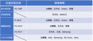
2000年後進入先進封裝世代,初期的晶片級封裝(Chip Size Package;CSP)仍是單晶片封裝,但尺寸不超過晶片面積的120%以符合電子產品輕薄短小的潮流。之後發展的系統級封裝(System in a Package;SiP)開始將多種功能晶片集成在單一封裝元件內,以較低成本達到如同系統級晶片(System On a Chip;SoC)的效用。接著推出的層疊封裝(Package on Package;PoP)是將兩個以上元件採垂直堆疊方式再封裝成更大的元件。後續發展的晶圓級封裝(Wafer Level Package;WLP)大幅改變製程,它先在晶圓上進行封裝、測試後再切割成元件,其尺寸等同晶片。2010年後朝向立體化發展,先後開發出2.5D與3D封裝技術。根據國際電機電子工程學會發布的報告指出目前各技術領導廠商如所表2所列。
Table 1: Leading Manufacturers of Advanced Packaging Technologies
Source : IEEE
1991年起由台灣、韓國、日本、美國和歐洲半導體協會資助成立的國際半導體技術發展藍圖(International Technology Roadmap for Semiconductors;ITRS)一直是引導產業往前邁進之指南,它預測在遵循摩爾定律下的半導體技術發展進程,不過在2016年發布的最後報告預估微處理器中電晶體尺寸將於2021年起停止微縮,等於宣告摩爾定律死亡,促使該組織中止運作。取而代之是由國際電機電子工程學會和國際半導體產業協會支持的異質整合藍圖(Heterogeneous Integration Roadmap;HIR),其認定的異質整合須滿足以下三個條件 :
- 封裝後體積必須變小:將不同功能的晶片與被動元件封裝成單一元件的體積必須比個別封裝的元件小。
- 必須整合不同類型的封裝技術:異質整合元件須應用不同類型的封裝技術,與單純將多個晶片封裝的技術不同。
- 必須包含各種類型的主動與被動元件:必須包含處理器、記憶體、邏輯元件、類比元件等數種晶片,甚至必須將被動元件、連接器、天線都封裝進去。
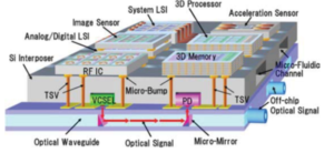
異質整合技術因為不需要透過印刷電路板連接,不僅能顯著減少系統體積與材料成本,還能依照不同應用場域的需求擴充晶片功能,且由於晶片之間的物理距離縮短,也能降低訊號傳輸過程中的消耗與降低傳輸所需的時間,一次滿足省電節能和效率提升的需求,故當前已成為半導體產業的主流技術。每年該組織會針對高性能運算和資料中心、醫療和穿戴式設備、自動駕駛汽車、行動通訊、航太和國防、物聯網等主要驅動異質整合技術進步的應用領域提出發展藍圖,並已確立系統級、晶圓級、2.5D/3D為異質整合的主要使用的封裝技術,詳述如下 :
圖1、採異質整合的自動駕駛車元件示意圖
Source : IEEE
- 系統級封裝(SiP) : 是基於系統單晶片發展的封裝技術,係從設計角度出發,把不同晶片以功能單元的方式集結設計在單一晶片中。而系統級封裝則是將多個不同功能的晶片或元件透過併排或堆疊等方式封裝單一元件。雖然系統單晶片整合的效能會比系統級封裝更高,但由於晶片的先進製程生產成本越來越高,加上產品功能多元化使得晶片設計日益複雜,且若為了整合進更多功能而增大晶片面積也會造成較低的生產良率。相較之下,由於製程技術難度較低,系統級封裝能夠大幅降低設計及製造成本,並可依照不同產品應用需求進行客製化,因此彈性及靈活度較大。
- 晶圓級封裝(WLP) : 傳統封裝方式都是先將晶圓上的晶粒切割成晶片後再進行封裝測試程序,而晶圓級封裝則是先在晶圓上進行大部分或全部的封裝測試程序,之後再切割成元件,若元件幾乎等同晶粒尺寸稱為WLCSP(Wafer Level Chip Scale Packaging)。它和印刷電路板的連接都是採用覆晶(Filp chip)形式,可達到最短的訊號導通路徑,具有更快傳輸速度和更少的寄生電感效應等優勢。目前該技術可分為扇入(Fan-In)與扇出(Fan-Out)等兩類型。最早推出是凸塊排列於晶片內的扇入型技術,但隨著尺寸持續縮小導致與印刷電路板連接的焊球難以容納於晶片面積內,如果將I/O接點或焊球縮小反而會降低生產良率,因此才衍生出扇出的封裝型態,它是在晶片範圍外的重構層(Redistribution Layer;RDL)製作導線以容納更多的I/O接點,還可連結各種不同功能的晶片或被動元件而整合在單一封裝體中,使其功能更加強大。由於扇出型晶圓級封裝能滿足高階晶片所需要的高I/O接點密度需求,又不需使用載板而可降低封裝厚度與成本,故吸引許多半導體大廠投入研發與量產。扇出型封裝的技術困難處是須克服異質材料間熱膨脹係數差異大和非對稱架構導致的晶片位移、晶圓翹曲等問題,以提升製程良率。
- 5D/3D封裝 : 2.5D封裝是將多顆晶片列排在矽中介板(Silicon Interposer)並用微凸塊連結,透過矽中介板傳導晶片訊號。3D封裝是將多顆晶片垂直堆疊並以矽穿孔(Through Silicon Via;TSV)與微凸塊連接,藉此減小彼此訊號傳輸路徑以增加處理與運算速度。過去一般封裝體內的晶片都是安裝在平面上,直到矽穿孔製程出現才讓封裝技術朝向立體堆疊方向發展。矽穿孔是在晶圓上以蝕刻或雷射鑽出小孔,再以金屬填補成導線以進行訊號的垂直互連,因此擁有更短的導通路徑而造就更低功耗、電阻與電感,讓訊號傳輸速度更快且雜訊干擾更小。矽穿孔的製程可分為先鑽孔(Via First)和後鑽孔(Via Last)兩類,前者是在晶片製程中以乾蝕刻技術完成矽穿孔,優點是能達到較小孔徑以具備較多I/O接點,但技術難度較高;後者是在封裝製程中以雷射鑽孔完成,優點是毋須改變晶片製程,缺點是孔徑較大而使得I/O接點密度無法提高。所有製程中以鍵合(Bonding)為關鍵步驟,是將晶片進行對準並接合以形成堆疊。以往推疊晶片是以微凸塊連接,隨著I/O接點間距往10μm以下發展後,半導體廠紛紛採用無凸塊(Bumpless)的混合鍵合(Hybrid Bond),透過高溫擴散方式讓兩晶片之矽穿孔的銅導線直接接合,可大幅增加I/O接點密度。因晶片緊密堆疊,須解決散熱不良問題以提高使用壽命。看好異質整合需求,當前全球半導體大廠都積極發展2.5D/3D封裝技術,例如:台積電的3DFabric平台、Samsung的Cube平台,Intel的EMIB、Foveros與Omni-Directional Interconnect (ODI)技術,日月光的VIPack平台,Amkor的SLIM與SWIFT技術。
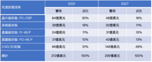
根據市場研究機構Yole Développement發布資料,2021、2027年前述先進封裝技術的市場規模如表3所列。2021年市場總和為213億美元,預估至2027年成長至299億美元,皆以2.5D/3D封裝的市占率最高且成長性最佳。
表2、2021、2027年各先進封裝技術市場規模與占比
Source : Yole Développement