異質整合專題|全球半導體封測產業發展動向剖析
Semiconductor packaging is a very fragile wafer wrapped in an outer shell and connected to the wire for use, so it has the effect of protecting the wafer, power supply, signal interconnection, heat dissipation and so on. The packaging industry is booming due to the continuous increase in wafer production, and is driven by the requirements for lightweight, thin, short, small, and high-performance electronic products, which have led to the continuous advancement of packaging technologies. According to a report released by ITRI IEK, benefiting from the Covid-19 epidemic triggered by the residential economy demand driven by the significant increase in the sales of communication products, the resulting chip shortage phenomenon pushed up the price of some packaging and testing products, making the global semiconductor packaging and testing industry in 2021, an annual increase in output value of 23.2%, amounting to 36.9 billion U.S. dollars. With the 5G communication, electric vehicles and other new technology market penetration rate continues to expand, so that the global packaging and testing output value to show growth, according to market research firm CINNO Research released data, the world's top ten outsourcing packaging and testing foundry (OSAT) in the first half of 2022, total revenue of 17.5 billion U.S. dollars, an annual increase of 16.7%, as listed in Table 1, of which five are Taiwan companies.
Table 1: Global Top 10 Outsourcing Foundries in the First Half of 2022
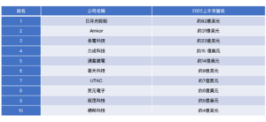
Source : CINNO Research
除了透過製程微縮以增加晶片的電晶體密度外,還須借助先進封裝技術才能製作出高性能的半導體元件,故近幾年隨著晶片製造邁入10nm以下製程,加上為降低生產成本而導入異質整合技術的晶片數持續增加,都帶動先進封裝技術迅猛發展,市場規模亦顯著擴大。根據市場研究機構Yole Développement發布的報告指出,2021年全球先進封裝市場規模為374億美元,預估2027年將成長至650億美元,年複合成長率為10%。全球前10大先進封裝廠商排名依序為日月光控股、Amkor、Intel、長電科技、台積電、Samsung、力成科技、通富微電、天水華天、UTAC,前6大廠商的總產量超過全球總額的80%。由於以往全球半導體產業著重在前段晶片製造領域發展,投入封裝的資源不多,導致委外封測代工廠技術發展進程無法配合投入先進製程的晶片製造商需求,於是它們率先切入先進封裝技術研發與生產,成為當前技術領導廠商,2021年台積電據有14%的全球產能,而Intel和Samsung合計占21%,其餘65%來自於眾多委外封測代工廠。2021年全球先進封裝的資本支出為119億美元,金額前五大廠商依序為Intel、台積電、日月光、Samsung、Amkor,顯示三大晶片製造商不但投資先進製程技術,也積極擴充先進封裝生產線。看好先進封裝的發展前景,吸引產業鏈上游的材料商與下游的專業電子代工商(EMS/ODM)切入該市場。例如欣興、Semco、AT&S和Shinko等載板廠商開發面板級封裝(Panel Level Package;PLP)技術並建置生產線,它是以玻璃、印刷電路板為載板進行封裝製程,由於基板面積大而能封裝更多晶片,故可降低生產成本。因為熟悉玻璃基板製程,如友達、群創、京東方、華星等面板廠正發展此業務,連Corning與AGC等玻璃基板供應商也開發專用載板。