
Industry Trend Report|Class III Semiconductor Trends in Electric Vehicle Applications
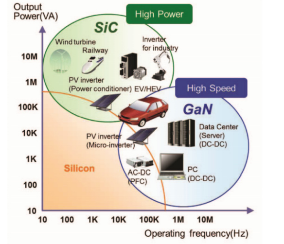
Currently, the operating voltage of commercially available EVs is around 300~400V, and the range can already reach the level of fuel vehicles, but the slow charging time is still the biggest pain point, prompting EV manufacturers to actively develop high-power fast charging stations. In order to match the use of EVs, it is inevitable to move to higher voltage development, after raising to 800V, it can greatly reduce the fast charging current and can use the lower price of small diameter high voltage wiring harnesses, and can optimize the use of efficiency due to less heat generation from batteries, so from 2021 onwards, there will be more than 800V models on the market. Nowadays, most electric vehicles below 600V use silicon-based MOSFET power components, while those above 600V use silicon-based IGBTs. However, during the power conversion process, the silicon-based power components that are subjected to high-voltage and high-current shocks are more prone to damage due to heat generation, and in order to solve this problem, some manufacturers have introduced wide-gap semiconductor materials, which provide power components with higher breakdown voltages and temperature tolerances. The result is power components with higher breakdown voltage and temperature tolerance, better reliability, faster switching speeds for high-frequency operation, and lower on-resistance for less power consumption, which are attracting more and more automakers to adopt them. Gallium nitride (GaN) and silicon carbide (SiC) are the most widely used wide-gap semiconductor materials. The main difference between the two is that SiC has a higher voltage resistance, which makes it suitable for electric vehicles, supercharging stations, transportation vehicles, and energy applications that require high voltage, whereas GaN has a faster switching frequency, which makes it suitable for consumer electronics, light-duty vehicles, hybrids, and 5G RF communication applications, as shown in Fig. 2. Some areas of the two overlap in electric vehicles. Generally, silicon carbide power components are selected for high voltage and high current applications above 600V, while gallium nitride power components are selected for medium voltage and high switching frequency applications below 600V. Despite the excellent performance of silicon carbide power components, they will not completely replace silicon-based IGBTs or MOSFETs due to their respective advantages in switching characteristics, power consumption, and cost, but will be developed in their own applications where they are well suited.
Fig. 2: Comparison of the characteristics of Si, SiC and GaN in terms of power output and switching frequency.
Source: IEEE
Silicon carbide has high collapse voltage characteristics. The power components made from silicon carbide can withstand high current density and operating temperature when used in high voltage systems such as inverters and on-board charging circuits, and have high-speed switching capability, which can provide higher reliability for electric vehicle systems. Currently, the main types of silicon carbide power components for EVs are MOSFETs and SBDs, with MOSFETs attracting attention because of their introduction into the inverter of the long range version of the Tesla Model 3. Because the voltage of 800V or more vehicles need to use 1200V power components, only silicon carbide can play this important role, with the increase in the penetration rate of electric vehicles in the future, it is expected to continue to expand its market, Fuji Economic estimates that by 2025 about 65.8% sales are in the automotive field. Silicon carbide SBD power components, on the other hand, are targeting vehicle chargers and fast charging piles as expansion markets, and are expected to account for 26.9% of sales in the automotive field by 2025. Yole Développement, a market research organization, reported that the global silicon carbide power components market will reach US$1.09 billion in 2021 and is expected to grow to US$6.29 billion in 2027. The automotive market, which accounts for the largest share of the market, is expected to grow from $690 million in 2021 to $4.99 billion in 2027, while the energy market, which accounts for the second largest share of the market, is expected to grow from $150 million in 2021 to $460 million in 2027. It is expected that the three major application markets in the future will be electric vehicles, PV and energy storage, and charging piles for electric vehicles; due to their inability to withstand crash voltages of 800V or more, GaN power components are better suited for use in electric vehicles. Gallium Nitride (GaN) power components are better suited for DC converters and low-power vehicle chargers because they cannot withstand breakdown voltages above 800V. However, because the technology is not as mature as that of silicon-based components and silicon carbide power components, the penetration rate in the automotive field is still low, and it is estimated that the automotive field will account for 21.2% of the company's sales by 2025. According to a report by Yole Développement, the global gallium nitride power component market will reach $46 million in 2020 and is expected to grow to $1.1 billion in 2026. The consumer market, which accounts for the largest share, is expected to grow from $29 million in 2020 to $670 million in 2026, and the automotive market is expected to grow from $0.3 million in 2020 to $160 million in 2026, according to Yole Développement.
Development Bottleneck of Silicon Carbide Power Components
Insufficient wafer supply has been one of the major bottlenecks limiting the development of silicon carbide power components. Currently, silicon carbide wafers are mainly grown by the physical vapor transport (PVT) method at a temperature of more than 2,300°C, while silicon wafers are grown at about 1,600°C. The high temperature greatly increases the difficulty in controlling the equipment and process. The high temperature greatly increases the difficulty in controlling the equipment and the process. If the temperature and pressure are not controlled correctly, the wafers that have been grown for several days will not be available for the subsequent process. In addition, the growth rate of silicon carbide in this method is slow, about 2cm in 7 days, while SiP can produce 2m 8-inch silicon wafers in 2~3 days; on the other hand, there are more than 200 crystalline structures of silicon carbide, but only the hexagonal structure of the 4H-type (4H-SiC) monocrystalline silicon carbide is a usable semiconductor material, and the growth process of the crystals needs to be precisely controlled in terms of the silicon to carbon ratio, the gradient of the growth temperature, the growth rate and the gas flow and pressure. During the crystal growth process, it is necessary to precisely control the silicon to carbon ratio, growth temperature gradient, crystal growth rate, and gas flow pressure, otherwise it is easy to produce unusable wafers. In the subsequent production of power components before the epitaxial step, the quality of which has a great impact on the performance of the components, generally at a high temperature of more than 1500 ℃, but the consideration of sublimation problems can not be more than 1800 ℃, resulting in epitaxial rate is slow.
The annual production capacity of silicon carbide wafers in the world is about 400,000~600,000 pieces in 2021. The inverter used in Tesla Model 3 requires 24 power modules containing two silicon carbide MOSFET power components, so each car uses a total of 48 silicon carbide power components, and on average, two Model 3s require one 6-inch silicon carbide wafer, which will consume the global total production capacity of about 1 million cars if delivered. If the delivery volume reaches one million vehicles, it will almost consume the total global production. Therefore, Infineon, STMicroelectronics, Rohm, and other power component manufacturers, which are actively expanding their silicon carbide business, have laid out their upstream wafer production capacity, and it is expected that the problem of insufficient supply may be solved only when 8-inch silicon carbide wafer production capacity is opened.
-For more information, please clickContact Us -
 Industry Trend Report|Electric Vehicle Semiconductor Market Status
 Industry Trend Report|5G Communication Market Trends and Challenges