Industry Trend Report|Technology Review and Bottlenecks in Semiconductor Development (Up)
According to a long-term study by market research firm IC Insights, consumer demand has had an increasing impact on the global semiconductor market since 2000, and in recent years new consumer electronics products such as smartphones, wearable devices, game consoles, smart speakers, smart homes, and tablet computers have been introduced to drive the global semiconductor market to continue to grow. By the World Semiconductor Trade Statistics Association (World Semiconductor Trade Statistics; WSTS) released information pointed out that personal computers, smart phones, automobiles, consumer electronics goods and other consumer products accounted for the overall semiconductor market sales accounted for as high as 86.9%. These products create efficient computing, 5G communications, The demand for new technologies created by these products, such as efficient computing, 5G communication, AI, and self-driving cars, has driven the semiconductor industry to continue to develop advanced process technologies.
圖1、2021年半導體終端市場銷售占比分布
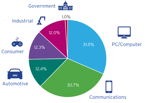
資料來源 : 世界半導體貿易統計協會
金氧半場效電晶體(Metal Oxide Semiconductor Field Effect Transistor;MOSFET)一直是主要採用的半導體元件,主要作用是訊號開關,由施加閘極的電壓大小決定電流能否自源極流向汲極。隨著電晶體尺寸縮小,源極和汲極間距離越來越近,當縮短到一定程度時會產生「漏電」現象,也就是即便不對閘極施加電壓,源極和汲極會出現導通的情況,此時電晶體失去開關控制的功能。過去很長一段時間,金氧半場效電晶體持續採用平面式結構,直到閘極寬度達到22nm時,已無法用任何方法避免發生漏電狀況,使得半導體製程發展陷入瓶頸。於是2011年Intel率先導入南加大胡正明教授研發出的鰭式電晶體,它是將源極和汲極拉高變成立體板狀結構,可增加源極與汲極間通道的表面積,樣一來即使寬度縮小到10 nm以下,閘極仍能控制源極流向汲極的電流,同時降低漏電和動態功率耗損。隨著深寬比不斷拉高,目前鰭式電晶體已逼近物理極限,為了製造出電晶體密度更高的晶片,2021年Samsung率先於3nm製程導入環繞閘極電晶體(Gate-All-Ground FET;GAAFET),台積電與Intel分別宣布將於2025、2024年量產的2nm製程採用。鰭式電晶體的源極與汲極間的通道是以三面和閘極接觸,而環繞閘極電晶體增加到四面,可再提升閘極對通道的控制能力,如圖1所示。台積電與Samsung的環繞閘極電晶體都採用納米片FET(Nanosheet FET)設計。
圖1、半導體使用的金氧半場效電晶體結構變化
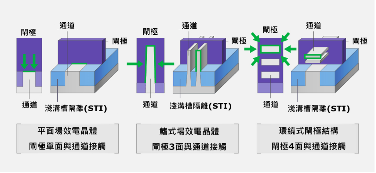
資料來源 : Samsung
當前全球半導體技術重量級研究機構比利時微電子研究中心(IMEC)正在開發2nm的Forksheet FET元件技術,與環繞閘極電晶體不同處是將NFET和PFET結合成一體,兩者以介電層隔離,可再縮小元件尺寸,如圖3所示。另外該機構還研發CFET元件技術,適用於1nm以下製程節點,它是將NFET和PFET堆疊在一起,使通道寬度可再擴大。通道可採鰭片或奈米片等形式,奈米片的CFET是金氧半場效電晶體的終極架構。不由於CFET結構較為複雜,所以發展出單片式(Monolithic)和序列式(Sequential)等兩種製程步驟,以後者的難度較低。
圖3、從FinFET到CFET的電晶體結構演進過程
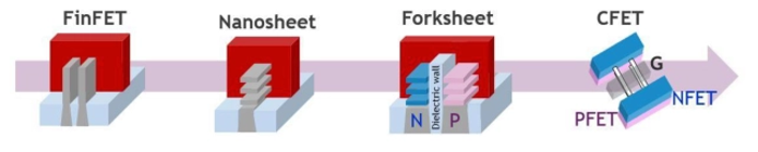
資料來源 : EE Times
上一篇:產業趨勢報告|Chiplet Revolutionizing Semiconductor Technology
下一篇:半導體發展之技術回顧與瓶頸 (下)
-For more information, please clickContact Us -
 Industry Trend Report|Technology Review and Bottlenecks in Semiconductor Development (Next)
 Industry Trend Report|Chiplet Revolutionary Semiconductor Technology