Industry Trend Report|Chiplet Revolutionary Semiconductor Technology
ChipletExploring the Dynamics of Technology Development
From the previous article, we have discussed that in order to reduce power consumption and improve performance in semiconductor transistors, semiconductor manufacturing processes continue to advance, and in addition to gate width shrinkage, the transistor has also changed from planar to three-dimensional. However, the production cost is also getting higher and higher, especially the Moore's Law, which is the guideline of the semiconductor industry, is gradually failing, and it is not possible to solve all the problems through process shrinkage. Therefore, Chiplet technology has become a solution to break through the bottleneck of Moore's Law, and reduce the cost of wafer development and manufacturing, which is to divide a single wafer into several functionally independent small wafers such as processor, analog components, memory, etc., and then integrate them into a functionally complete wafer by means of advanced packaging. It is a solution that divides a single chip into several functionally independent chips, such as processor, analog components, memory, etc., and finally integrates them into a full-featured chip through advanced packaging. The concept originated from Intel co-founder Gordon Moore's 1965 paper "Cramming More Components Onto Integrated Circuits," which not only proposed the famous Moore's Law, but also pointed out that it would be more economical to build large systems with small, single-function chips that are individually packaged and interconnected. In 2015, Marvell's Dr. Hsiu-Wen Chou proposed the concept of Modularized Chip (MoChi) at the International Solid-State Circuits Conference (ISSCC), which made the semiconductor industry pay attention to the Chiplet technology, and in recent years, in order to reduce the development and manufacturing costs of high-end chips, coupled with the rapid advancement of packaging technology, more and more IC designers have introduced the Chiplet design, which has become an important semiconductor industry trend. Chiplet design has become an important trend in semiconductor technology development and is changing the ecology of the global semiconductor industry. According to a report published by Omdia, the global Chiplet market is expected to grow from $5.8 billion in 2024 to $57 billion in 2035, and Chiplet technology has the following three advantages.
- Chipletization of SoCs allows each chiplet to be manufactured with the appropriate process technology and then integrated into a single SOC chip through advanced packaging technology, eliminating the need for front-end advanced manufacturing processes, which significantly reduces the cost of wafer production.
- Smaller wafers usually have fewer defects and better wafer area utilization efficiency, so SoCs can significantly improve process yields and reduce production costs after being Chipletized.
- Chipletizing SoCs enables selective updating of specific cells, which reduces repetitive design and verification efforts, thereby reducing the complexity and cost of chip design and shortening new product development time.
Fig. 1, Chiplet architecture schematic diagram
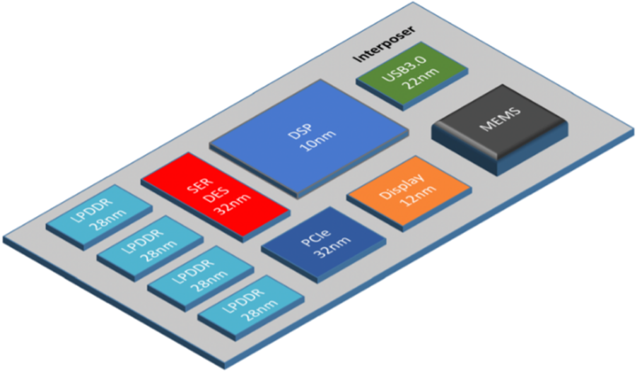
Source : Cadence
AMD是最先導入Chiplet技術的晶片公司,自2019年起全面採用該技術而提升產品市場競爭力。在2020年國際固態電路研討會上發布基於Zen 2架構的CPU產品,即將CPU與 I/O控制晶片分別使用不同製程技術,前者使用台積電的7nm製程,後者使用GlobalFoundries的14/12nm製程,兩者再以稱為Infinity Fabric On-Package(IFOP)封裝技術連接,該公司評估採用Chiplet的產品製造成本可減少50%。2021年AMD發表採用3D Chiplet設計的Ryzen9 5900X處理器,它是在配置的32MB SRAM的CPU上,透過台積電的SoIC先進封裝技術連接另一顆64MB SRAM,藉此讓Cache容量提高至96MB以增加運算效能。採用 3D Chiplet 的Ryzen 9 5900X平均每秒可處理的影像幀數比標準版多出12%。2022年AMD推出基於Zen 4架構的Ryzen 7000系列桌上型CPU,四顆產品都使用Chiplet設計,另外推出主機板用X670和X670E晶片組亦採用Chiplet設計,稱為Promontory 21(PROM21)晶片組,由祥碩科技(ASMedia)負責構建;為了挽回市場競爭頹勢,Intel也開始導入Chiplet技術,在2022年國際固態電路研討會上公布為Aurora超級電腦開發的Ponte Vecchio GPU技術細節,它由63個Chiplet連接而成,總堆疊面積為 3,100平方毫米,共含1,000億個電晶體。
為了推動Chiplet技術發展,2022年台積電、日月光、Intel、AMD、ARM、Google Cloud、Meta、Microsoft、Qualcomm、Samsung等公司共組UCIe (Universal Chiplet Interconnect Express)產業聯盟,目前推出UCIe 1.0規範,提供包含物理層、堆疊、軟體模型和測試等完整的標準化晶片到晶片(Die to Die)互連規範,讓終端使用者打造SOC晶片時能自由搭配來自多個生態系廠商的Chiplet產品。未來將著手制定下一代UCIe規範,包含Chiplet外型、I/O管理、安全性和其他必要之協定。
雖然採用Chiplet技術可省去使用前段先進製程而降低晶片生產成本,但是因為須採用複雜的先進封裝技術,所以未必能達到預期的成本縮減效果。根據中國清華大學交叉資訊研究所發布論文指出,以14nm、7nm、5nm等節點製程及SoC、MCM、InFO、2.5D等封裝技術為研究範疇,其結果顯示當前段製程下降至5nm節點與面積超過800 mm2的大尺寸晶片使用Chiplet技術才具成本效益,也就是在前段製程越接近摩爾定律極限與多晶片架構的情況下才需採用Chiplet技術。
Chiplet發展對封裝產業影響分析
由於Chiplet概念的實踐必須仰賴先進封裝技術,故將是其盛行下的最大受益者。目前投入先進封裝的廠商分為晶圓代工廠和委外封測代工廠(OSAT)等兩大陣營,前者主要在矽晶圓上製作互聯導線,以提供更高速的連接和更好的應用彈性;後者則努力減少矽晶圓上製程需求,以提出更有性價比的方案。因為晶圓代工廠對前段先進製程所製造的晶片掌握度高,且研發人才及資源較為豐沛,故逐漸成為先進封裝技術主導者,重要的先進封裝廠商技術發展現況詳述如下 :
- 台積電 : 2020年推出3DFabric先進封裝平台,前段為使用Hybrid Bonding製程的SoIC技術,後段則採用成熟的2D/2.5D的InFO技術及5D的CoWoS技術,其中CoWoS技術包含CoWoS-S、CoWoS-R及CoWoS-L等三種封裝方式,CoWoS-S是以矽中介層連接Chiplet,因為其面積大可提供更高密度的晶片連接,但生產成本較高。CoWoS-R是使用有機中介層連接晶片,其與部分封測廠提供的方式一致,它的連線密度較低但可降低生產成本。CoWoS-L是使用內嵌矽橋的有機中介層連接晶片,其連線密度與生產成本介於CoWoS-R和CoWoS-S之間。InFO技術包含InFO_OS、InFO_LSI等兩種封裝方式,主要差異是後者適用於LSI晶片封裝,因LSI的高運算速度與高頻寬需求而採用導線更細的RDL及更小的凸塊間距。
- Samsung : 2020年發布X Cube 3D封裝技術,晶片以矽通孔連接,目前已經能把SRAM晶片堆疊在7nm製程的邏輯晶片上,可易於擴充Catche容量,同時縮短信號連接距離以提升資料傳輸的速度和效率。
- Intel : 推出5D封裝的EMIB與3D封裝的Foveros等先進封裝技術,目前凸塊間距各為36~55μm及25~50μm,每平方毫米可容納的最大凸塊各為1,100顆與1,600顆。2020年發表混和接合技術Co-EMIB,即是利用EMIB將多個已經完成堆疊封裝的Foveros晶片模組串接起來,再安置於同一個載板上,以實現更大型、更複雜的多晶片整合系統。晶片垂直堆疊則提出Omni-Directional Interconnect (ODI)技術,藉由在微銅柱來實現晶片與基板的互聯,可省去TSV占用的空間。未來預計改用無凸塊的Hybrid Bonding技術,適用於10μm以下接點間距,可提供更高連接密度與頻寬、更低的功耗。
- 為因應3D異質整合需求,2022年日月光推出VIPack先進封裝平台,提供垂直互連整合封裝解決方案,此平台利用RDL製程、嵌入式整合及5D/3D封裝技術,協助客戶在單個封裝中集成多個晶片來實現創新未來應用。它是六大核心封裝技術组成,包括Fan Out Package-on-Package (FOPoP)、Fan Out Chip-on-Substrate (FOCoS)、Fan Out Chip-on-Substrate-Bridge (FOCoS-B)、Fan Out System-in-Package (FOSiP),以及矽通孔的2.5D/3D封裝和Co-Packaged Optics。
- Amkor推出無矽通孔的SLIM及SWIFT等先進封裝技術,所以製程難度較低,可實現多晶片的3D POP封裝,適用HPC、FPGA與Mobile AP等產品。
先進封裝是Chiplet技術核心之一,由於難以標準化而呈現出百花齊放的局面,於是UCIE聯盟並未嚴格限制封裝方式,根據發佈的Chiplet白皮書內容顯示,該聯盟支持市面上四種主流封裝技術,包括:(1).將晶片間的金屬導線埋入封裝載板中的標準封裝;(2).利用矽橋連接晶片,並將其嵌入封裝基板中,如Intel的EMIB技術;(3).使用矽中介層連接晶片並進行重新佈線,再將其嵌入到基板上,如台積電的CoWoS技術。(4).使用扇出型中介層進行重佈線,僅在晶片連接處使用矽橋連接,如日月光的FOCoS-B技術。
面對前段先進製程成本不斷墊高的壓力,考量後段先進封裝技術難度與產線投資額相對較低,卻可帶來更顯著效益,故成為半導體製造商積極布局之處。根據創投公司Insight Partners發布報告指出,預估全球先進封裝市場規模將從2020年的300億美元成長到2028年的550億美元,其占整體封裝市場比例也將從2020年的40%增長至2030年的60%。目前Intel、Samsung、台積電、日月光、矽品、Amkor、力成、長電、頎邦、Nepes等十家廠商在先進封裝市場合計占有率達75%。
另根據市場研究機構Yole Développement發布的報告指出,預估全球先進封裝市場規模將從2020年的300億美元成長到2026年的475億美元,2020~2026年複合成長率為8.0%。各分項技術的市占率變化如圖2所列,其中以Chiplet較常使用的3D Stocked技術市占率由2020年9%擴張至2026年19%之幅度最大。雖然委外封測代工廠據有較高的先進封裝市占率,但高階的2.5D/3D堆疊、高密度Fan-Out等先進封裝技術逐漸由晶圓代工廠取得主導地位,並推動封裝施作環境從載板轉移到晶圓或矽平台。另一方面,隨著先進封裝市場快速擴大,正吸引晶圓代工廠和委外封測代工廠以外的載板與PCB供應商、電子專業製造廠(EMS)投入此領域,雖然市場會因為新進者加入而更競爭,但也代表商機無限。
圖2、2020、2026年各先進封裝技術市占率變化
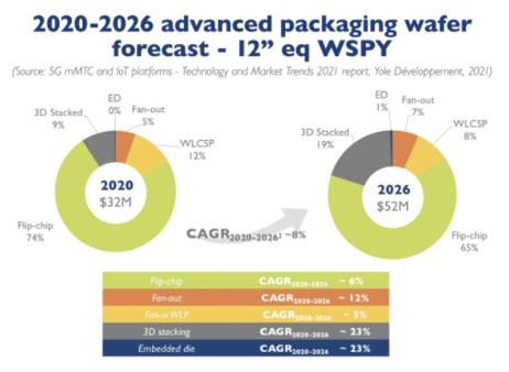
Source : Yole Développement
上一篇:產業趨勢報告 | Type C一統趨勢下,供應鏈的韌性分析
下一篇:產業趨勢報告|半導體發展之技術回顧與瓶頸 (上)
-For more information, please clickContact Us -
 Industry Trend Report|Technology Review and Bottlenecks in Semiconductor Development (Up)
 Industry Trend Report|Type C Unification Trend, Supply Chain Flexibility Analysis