Industry Trend Report|Technology Review and Bottlenecks in Semiconductor Development (Next)
Micrographics is a key process for determining the size of a component, and the exposure machine that creates the circuit pattern on the photoresist is the core equipment. According to the Rayleigh Criterion formula, the minimum linewidth that can be exposed is directly proportional to the wavelength of the light source used in the exposure machine (λ) and inversely proportional to the numerical aperture (NA). Table 1 shows the development of exposure machine technology. Currently, there are only three manufacturers in the world that are capable of developing exposure machines for semiconductor front-end wafer fabrication, namely Nikon, Canon and ASML. At that time, almost all of the exposure machines used by Intel, the leading semiconductor company, were customized by Nikon, while TSMC and Samsung were still small companies in the semiconductor industry, and ASML was just a newly established exposure machine manufacturer. Because the resolution of ArF light source is limited to 65nm, Nikon and Canon chose to develop an exposure machine using a shorter wavelength 157nm light source in order to enable semiconductor front-end processes to move to smaller sizes, but unfortunately encountered major difficulties and failed. ASML not only solved the bottleneck of semiconductor process, but also could be used up to 7nm process with multi-exposure technology. ASML has since become the dominant semiconductor pre-processing exposure machine in terms of market share, and is currently the only company in the world that has the capability to develop and manufacture extreme ultraviolet (EUV) exposure machines. In response to the demand for sub-3nm nodes, ASML and Microelectronics Research Center (MRC) are collaborating on the development of a high-NA EUV exposure machine, which is expected to be launched in 2024, just in time to meet TSMC's and Intel's 2nm mass production schedule. In addition to exposure machines, the Microelectronics Research Center is also developing new photoresist and photomask films for particle contamination prevention. The continuous shrinkage of components increases the difficulty of film coverage and etching, for which equipment vendors have introduced atomic layer deposition (ALD) and atomic layer etching (ALE) equipment, the former of which uses a single layer of atoms to form the film by deposition, and the latter of which uses a single layer of atoms to remove the film by removal. ALD and ALE equipment is only applicable to inorganic materials. As more and more organic materials are introduced into advanced processes, equipment vendors are developing molecular layer deposition (MLD) and molecular layer etching (MLE) equipment, and are also working on the ability to selectively deposit or etch the aforementioned equipment, which reduces the number of micrographic process steps and reduces the amount of equipment to be purchased.
表1、曝光機技術發展歷程

資料來源 : 智璞產業趨勢研究所整理
由於半導體先進製程研發難度與產線建置費用非常高,使得Intel以外的IDM廠商在矽半導體領域都紛紛放棄既有營運模式,將高階晶片交由台積電、Samsung、聯電、GlobalFoundries、中芯國際等晶圓代工廠生產,這些公司的製程技術節點發展狀況如表2所列,目前僅台積電與Samsung有能力生產5nm以下節點晶片,另外如表3所列,隨著投入先進製程的半導體製造商大幅減少,使得極少數技術領先的晶圓代工廠逐漸掌握晶片製造議價權,如台積電在市況不佳時還調漲代工價格,為了穩固日後產能絕大部分客戶都會買單。
過去半導體產業是根據電晶體的閘極長度來決定製程節點,但當平面電晶體結構轉變為立體的鰭式電晶體後,評量晶片製程技術優劣時必須考慮到鰭的間距、寬度或高度,以及電晶體密度,而且它的效能及可微縮面積都較傳統電晶體大幅提升,故製程進入22nm後就節點數只是象徵半導體廠製程技術的演進狀況,無法直接評斷其技術能力,比較有說服力的指標是電晶體密度。以技術領先的台積電、Samsung與Intel為例,根據市場研究機構Digitimes發布資料,在10nm節點,Intel的電晶體密度為每平方毫米1.06億顆,是台積電和Samsung的兩倍。在7nm節點,Intel的電晶體密度為每平方毫米1.8億顆,台積電與Samsung各為 9700、9500萬顆,Intel還是台積電和Samsung的兩倍。而在5nm節點,預計Intel的電晶體密度為每平方毫米3億顆,台積電與Samsung各為1.73、1.27億顆,Intel仍舊是台積電和Samsung的兩倍。故Intel的10nm、7nm製程分別相當於台積電和Samsung的7nm、5nm製程。在3nm節點,台積電與Samsung的電晶體密度各為每平方毫米2.9、1.7億顆,所以台積電與Samsung各相當於Intel的5nm、7nm製程,由此可知Intel居半導體技術領導地位。另一方面,自5nm節點後,Samsung的電晶體密度明顯低於台積電,顯示其製程能力居於劣勢,所以Apple、AMD、Qualcomm、Nvidia、Broadcom與聯發科等IC設計大廠都有在台積電投產高階晶片,Samsung只能靠低價爭取部分公司訂單。
表2、重要晶圓代工廠的製程技術節點發展狀況

資料來源 : 智璞產業趨勢研究所整理
表3、參與各前段製程技術節點的晶片製造商與曝光機廠商

資料來源 : CSET
由於矽半導體前段製程已逼近物理極限,大幅提升其製程複雜度,進而導致生產成本大幅提升,根據喬治城大學沃爾什外交學院安全與新興技術中心(Center for Security and Emerging Technology;CSET)發布的報告指出,估算台積電每片晶圓的生產成本自90nm的1,627美元增加至7nm的9,213美元與5nm的16,746美元,而每片晶圓的代工報價自90nm的1,650美元增長至7nm的9,346美元與5nm的16,988美元,故5nm與7nm分別是90nm的五倍、十倍,而5nm竟然是上代7nm的兩倍。另一方面,生產成本昂貴的先進製程也顯著提高晶片開發成本,根據市場研究機構International Business Strategies發布的報告指出,晶片開發成本自65nm的2,850萬美元成長至5nm的5.42億美元,使得只有大型IC設計公司才有能力開發先進製程製作的晶片產品。從晶片效能的角度來看,2000年前每隔1.57年就可讓中央處理器效能出現翻倍成長,但近幾年摩爾定律逐漸失效,翻倍提升時間延長至2.6年,圖4是台積電、Samsung與Intel之相鄰製程節點間電晶體效能提升比率變化狀況,顯示10nm節點後提升幅度變小。由前述內容可得知先進製程投資金額高但已無法製作出效能更顯著的晶片。
圖4、相鄰製程節點間電晶體效能提升比率變化
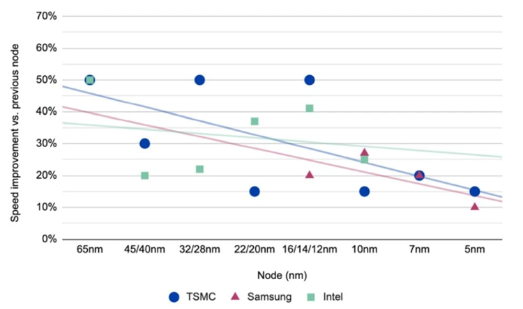
資料來源 : CSET
上一篇:產業趨勢報告|半導體發展之技術回顧與瓶頸 (上)
下一篇:發表會 | 2023年重要科技趨勢 (下)
-For more information, please clickContact Us -
 Seminar|Key Technology Trends in 2023 (Next)
 Industry Trend Report|Technology Review and Bottlenecks in Semiconductor Development (Up)