先進封裝設備材料專題|2.5D/3D 封裝之重要性與關鍵的製程點(上)
2.5D/3DWhy is packaging the mainstay of wafer fab production and why is it important?
Since the world's first integrated circuit was born in 1958, the performance of chips has depended on transistor miniaturization. However, as device size approaches its physical limits, process node is becoming a commercial marketing term. Using advanced processes to shrink devices no longer brings cost reductions, but rather increases costs significantly due to the difficulty of shrinking. As the demand for transistor density and chip performance continues to rise, advanced packaging technology has become an important solution. Advanced packaging technology shifts the wafer architecture to a combination of horizontal and vertical stacking of more wafers, which becomes a necessary technology to continue Moore's Law.
Conventional packaging is a combination of flat type wire bonding and
圖一、晶片成本隨著技術節點微縮而增長
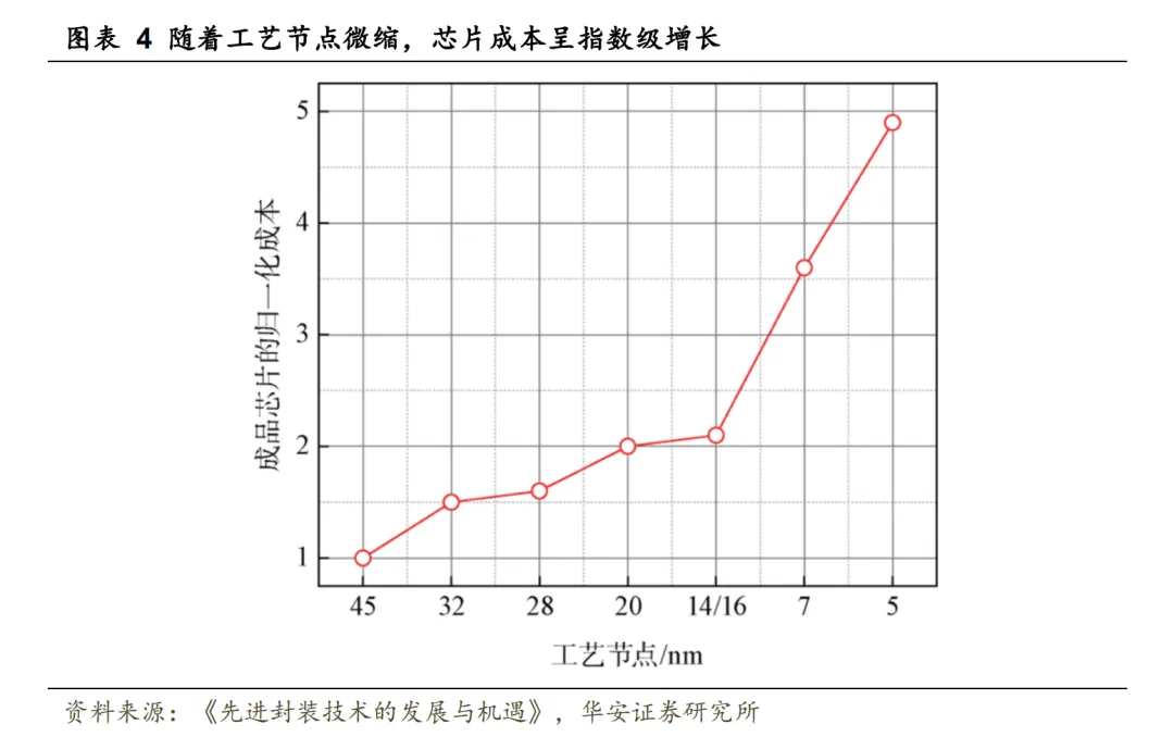
資料來源:華安證券研究所
先進封裝技術通常會是異質整合的,其中包括 3D IC、2.5D IC、扇出晶圓級封裝/面板級(如九月專題)、系統級封裝、絎縫封裝等。由於目前AI/高算(HPC)需求以2.5D/3D IC為主,近兩年將會是以此解決方案為主流,因此我們聚焦於此。2.5D/3D IC主要是將晶片猶如積木一般向外與向上堆疊並封裝成型,使晶片節省能耗與成本,還能夠提升計算效率。在技術概念上 2.5D 與 3D 封裝技術則是差別在堆疊方式,如下圖二。2.5D 封裝是指將晶片堆疊於中介層之上或透過矽橋連結晶片,以水平堆疊的方式,主要應用於拼接邏輯運算晶片和高頻寬記憶體;3D 封裝則是垂直堆疊晶片的技術,主要面向高效能邏輯晶片、SoC 製造。以台積電為例,2.5D技術發表約10年,但由於過往該技術較昂貴較少被提及,反而是成本相對低的InFO封裝較受關注。近年來,2.5D/3D憑藉著其極高的封裝密度和能源效率的優勢,作為最理想的晶片整合平台並獲得了發展勢頭。
圖二 2.5D與3D封裝示意圖
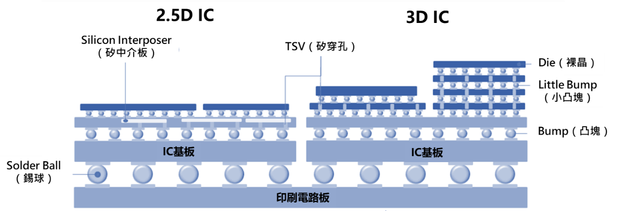
資料來源:台積電官網;智璞產業趨勢研究所整理,2024/11
根據Mordor Intelligence的報告指出,2.5D/3D的半導體封裝市場規模預計從2024年的97.9億美元,於2029年成長至216.3億美元,在預測期間內的年複合成長率為17.2%,而其中成長最快以及最大的市場皆為亞太地區(如圖三)。
圖三、2.5D及3D半導體封裝產業市場規模
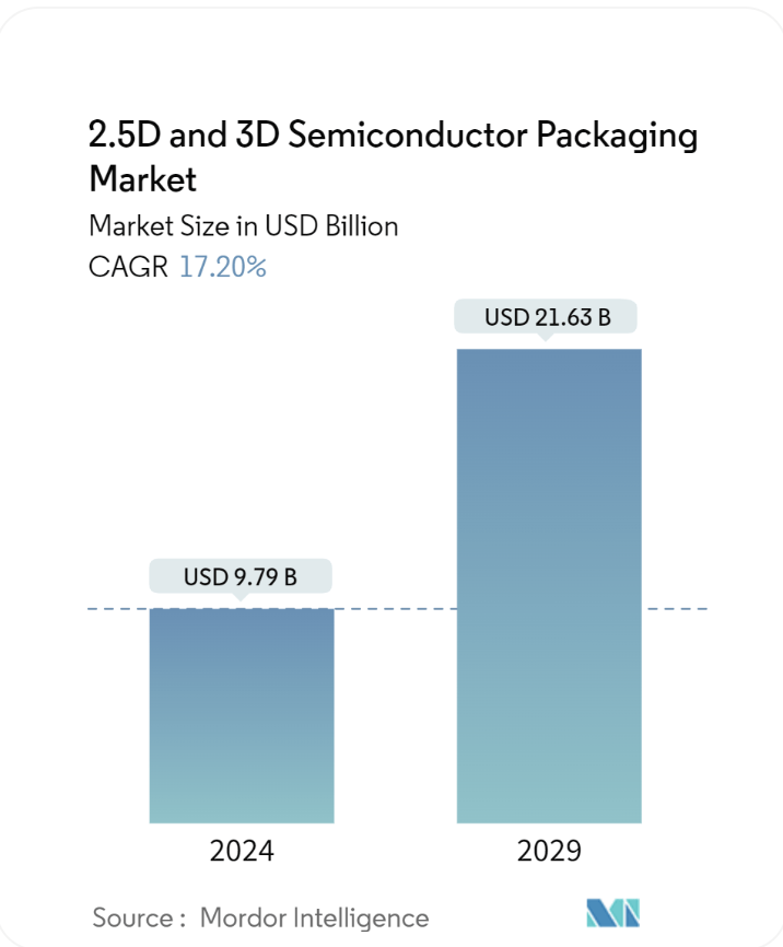
資料來源:Mordor Intelligence