August_Semiconductor|Advanced Packaging Technology for High Performance Computing Chips(M)
According to the Heterogeneous Integration Technology Blueprint report released by IEEE, short-term HPC chips are linked to other chips by large-area intermediary layers, embedded bridge carrier boards, small-aperture-ratio silicon through-holes, face-to-face wafer stacking, and hybrid bonding, etc., as illustrated in the following.
- Large Intermediate Layer: This is the mainstream 5D packaging technology for HPC chips. Four HBMs are usually connected through the intermediate layer, but as chip performance continues to increase, a larger intermediate layer will be needed to accommodate up to eight HBMs.
- Embedded Bridge Layer: A bridge layer made of silicon or glass is embedded in the carrier board and bonded to the chip and the carrier board through two side pillars to replace the silicon intermediary layer. The current adopters are Intel's EMIB and Sun Micron's FOCos-Bridge technology [discussed in detail in the previous article:Chiplet Revolutionizing Semiconductor Technology ]. When the placement accuracy is greatly improved, it is expected that the carrier board can be embedded with multiple bridge layers as an alternative to the conventional 5D package.
- Small aperture silicon vias: At present, the depth and width of silicon vias for interlayer silicon is usually 100μm:10μm, while the depth and width of silicon vias for stacked DRAM and logic wafers are 50μm:6μm and 50μm:5μm, respectively. After the introduction of a large number of 3D packaging technologies, the silicon vias have to be continually shrunk in order to increase the density of I/O points. It is estimated that the depth-to-width ratio will remain at 10:1.
- Face-to-face wafer stacking: Currently, the top and bottom wafers are mainly bonded by tin-lead micro bumps. However, in order to increase the density of I/O points, such as Intel's Foveros-Direct technology, a smaller and lower resistance copper pillar is used, which reduces the pitch of the joints up to 10 μm.
- Hybrid Bonding: This is a process in which the metal and oxide mixed interfaces on both sides of the wafer are directly bonded and then allowed to diffusely bond at high temperatures. Because the process mainly uses wafer fabrication equipment, it can reduce the contact spacing to the sub-micron level, and is regarded as the key technology for realizing true 3D packaging. It has been widely used for bonding CMOS image sensors to logic chips and memory, and is being introduced into high-performance computing chip packaging, such as TSMC's SoIC technology.
In addition, the report identifies medium- and long-term technology development directions for advanced packaging for HPC chips, including ultra-fine-pitch carrier boards, wireless on-chip communications, and silicon-photonics solutions, as follows.
- 超細間距載板:為了取代價格較高的矽中介層,多家供應商正在開發線寬與線距為1~2μm的載板,然而受限於製程難度高且可靠度達標不易,目前仍無法量產。若能突破前述困難而量產,生產成本將成為能否大量導入的關鍵。
- 無線晶片通信:利用晶片I/O點間電感耦合有潛力取代晶片間連接用矽通孔,以降低中介層或載板的佈線複雜度。然而需要針對如基板電阻率、晶片厚度等參數對電感耦合效應及各種工作頻率下對 I/O點訊號質量之影響進行深入研究,以確保其實施之可行性與穩定度。
- 矽光子解決方案:一般光電模組包含光接收器、放大器、調變器等元件,以往是放在電路板上,矽光子技術則整合到矽晶片上。目前封測廠正在發展的共封裝光學模組(Co-Packaged Optics;CPO)技術主要將電子和光子積體電路封裝在單一載板上以減少傳輸耗損及訊號延遲。
如前所述,先進封裝技術藍圖之推進處在於縮減線寬與線距、鍵合點間距,所以微影與鍵合為其關鍵設備。根據市場研究機構Yole Développement發布報告指出,2020年全球先進封裝用微影與鍵合設備市場規模為17億美元,預估2027年成長至28億美元,年平均複合成長率達8%,如圖4所示,個別設備說明如下:
- 先進封裝用微影設備:全球市場規模將從2020年的13億美元增長至2027年的19億美元,年平均複合成長率達5%。主要供應商有EVG、SUSS、Canon、Nikon、ASML、Veeco、ONTO、Hakuto、USHIO、ORC、Kulicke & Soffa、Orbotech、ORC、SCREEN、ADtech、SMEE、Heidelberg Instrument。
- 永久鍵合設備:全球市場規模將從2020年的61億美元增長至2027年的5.07億美元,年平均複合成長率達16%。主要供應商有EVG、SUSS、Canon、TEL、Nidec、AML、SMEE、Bondtech、Ayumi。
- 暫時鍵合設備:全球市場規模將從2020年的13億美元增長至2027年的1.76億美元,年平均複合成長率達7%。主要供應商有EVG、SUSS、TEL、SMEE、Tazmo、TOK、Takatori、EO Technics、ERS Electronic。
圖4、2020~2027年先進封裝用關鍵設備市場規模變化
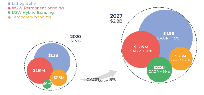
Source : Yole Développement
根據國際半導體產業協會(SEMI)與市場研究機構TECHCET共同發表的「全球半導體封裝材料市場展望」報告指出,受惠於先進封裝技術強勁需求,預期帶動全球半導體封裝材料市場規模自2022年261億美元擴增至2027年的298億美元,年平均複合成長約2.7%,其中約60%來自於載板。台灣電路板協會的統計資料指出,2022年台灣是全球最大的載板產地,產值占比達38.3%、其次為韓國與日本,三地廠商總計囊括九成的市場。全球前五大供應商為欣興、南亞電子、Ibiden、SEMCO、Shinko,市占率分別為17.7%、10.3%、9.7%、9.1%、8.5%。
 August_Semiconductor|Advanced Packaging Technology for High Performance Computing Chips(Up)August_Semiconductor|Advanced Packaging Technology for High Performance Computing Chips(Next)