August_Semiconductor|Advanced Packaging Technology for High Performance Computing Chips(Up)
With the transistor size shrinkage gradually approaching the physical limit, resulting in advanced manufacturing process difficulties and lead to rising wafer production costs. For a fab with a capacity of 50,000 wafers per month, it is estimated that the cost of building a fab since the 14nm process will exceed $10 billion, and the cost of a 5nm process fab will increase by 60% to $16 billion. In addition to the significant increase in fab costs, the operation and maintenance costs after mass production are also very alarming. The Center for Security and Emerging Technology (CSET) estimates that the cost of manufacturing each wafer has decreased from $331 for 12/16nm process to $233 for 7nm process, but increased to $238 for 5nm process. This means that the previous method of increasing throughput by reducing wafer size through advanced processes to reduce production costs is no longer applicable, and the performance improvement of transistors has been declining [discussed in more detail in the previous article:Technology Review and Bottlenecks in Semiconductor Development]This means that the semiconductor industry is facing the dilemma of having to invest very high amounts of money in advanced processes but not being able to produce more significant wafers. This means that the semiconductor industry is facing the dilemma of having to invest a very high amount of money in advanced processes, but not being able to produce chips with more significant performance. As a result, some of the R&D centers of semiconductor manufacturers are gradually shifting to advanced packaging to break through the dilemma.
傳統封裝是先將晶圓片切割成晶片再各別進行封裝的技術,晶片是透過銲線(Wire Bond)連接導線架或載板。先進封裝通常是在晶圓完成封裝製程後再切割成元件,晶片是用Bump或Pillar與其他晶片、中介層、載板連接,如圖1所示。
圖1、傳統封裝與先進封裝製程差異示意圖
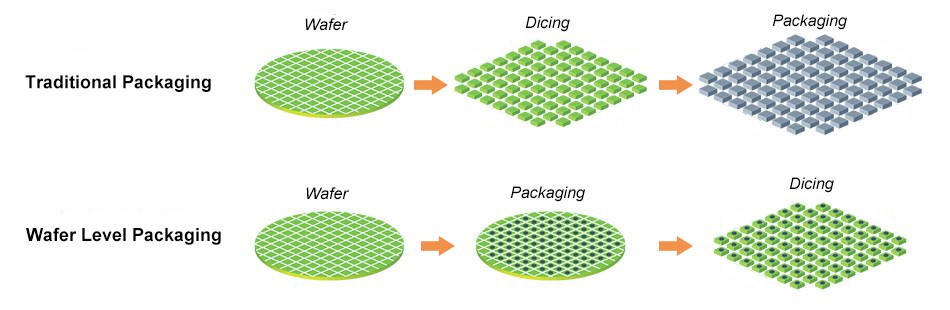
資料來源 : Semiconductor Engineering
根據市場研究機構Yole Développement發布的報告指出,2022年全球先進封裝市場規模約為443億美元,占整體封裝市場份額為44%。預估2028年將成長至786億美元,市場占比首次超越傳統封裝而達到52%,年平均複合成長率為10%。就應用領域來看,先進封裝技術主要用於手機和消費性電子產品,2022年占比高達70%,預估至2028年小幅下降至61%。第二大應用是通訊與基礎設施,預估占比自2022年的20%成長至2028年的27%。第三大應用是運輸,估計占比自2022年的6%增長至2028年的9%,如圖2所示。
圖2、2022~2028年全球先進封裝應用占比變化
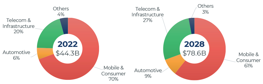
Source : Yole Développement
目前投入先進封裝領域的業者包含晶片製造商、委外封測(OSAT)代工廠與載板製造商。在晶片製造商部分,當前全球僅有台積電、Intel與Samsung能夠量產7nm以下先進製程晶片,故研發能力領先其他半導體業者,都相繼將晶片製造的技術能量與優勢投入先進封裝領域。2022年台積電投入25~35億美元於先進封裝領域,繼2020年整合3D封裝之SoIC與2.5D封裝的InFO及CoWoS等技術推出3D Fabric平台後,2022年成立3D Fabric聯盟並有19家夥伴廠商加入,2023年6月首座導入3DFabric平台的苗栗竹南廠啟用,是台積電第6座先進封裝廠。Intel在2022年資出30~40億美元於先進封裝領域,計劃在美國新墨西哥州、馬來西亞廠區擴增產能,並在義大利建立新廠。Samsung在同一年投入10~20億美元於先進封裝領域,並設立半導體封裝工作小組以強化該業務發展,2023年延攬台積電前研發副處長林俊成擔任該小組副總裁,負責先進封裝技術開發工作。
在OSAT部分,日月光控股、Amkor、長電科技等全球領導業者正積極拓展先進封裝業務。2022年日月光控股的資本支出約為18億美元,超過一半用於封裝領域,同年推出六種技術組成的VIPack先進封裝平台。2022年Amkor資本支出為9.5億美元,主要用在越南新建系統級封裝(SiP)生產線,已推出無矽穿孔(TSV-less)的Silicon-Less Integrated Module(SLIM)及Silicon Wafer Integrated Fan-out Technology(SWIFT)等解決方案。2022年長電科技的資本支出約為8.4億美元,也採用無矽穿孔技術路線,2021年發布XDFOI解決方案,涵蓋2D、2.5D和3D封裝技術;在載板製造商部分,Semco、欣興電子、AT&S和Shinko等廠商利用其專業知識與產能跨足面板級扇出型封裝(FOPLP)、嵌入式裸晶等先進封裝領域,前者有Semco、欣興電子,AT&S則是後者的重要業者。根據市場研究機構Yole Développement發布的報告指出,2022年全球前十大先進封裝廠商依序為日月光控股、Amkor、Intel、台積電、長電科技、Samsung、通富微電、力成科技、天水華天、智路封測,如表1所列。2022年名單與排名順序和2021年相同,其中成長性最高的前三名廠商是通富微電、台積電與Samsung。
表1、2022年全球前十大先進封裝廠名單
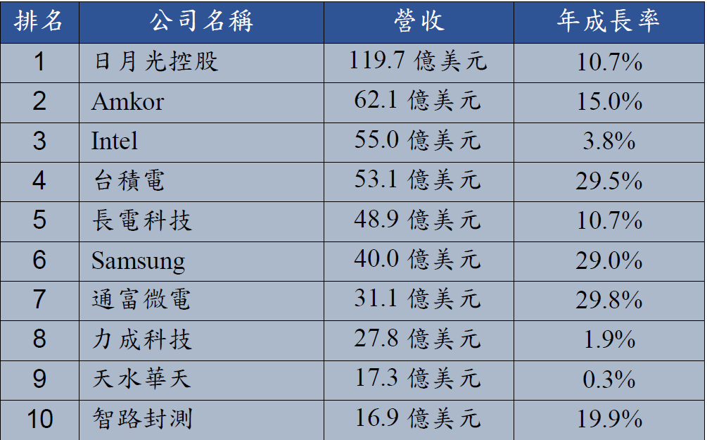
Source : Yole Développement
近年來由於政府資金大舉投注半導體產業,使得中國廠商透過併購或入股外國公司而快速崛起,並取得先進封裝技術。如2015年長電科技收購新加坡STATS ChipPAC、2016年通富微電收購AMD位於中國蘇州和馬來西亞檳城的封測廠、2019年天水華天收購馬來西亞Unisem股權,資產管理公司智路資本相繼於2020年收購新加坡UTC、2021年收購力成科技的新加坡凸塊廠,以及2022年收購日月光控股位於中國上海、蘇州、昆山、威海的封測廠。由於目前中國封裝廠商未落入美國半導體制裁範圍內,預期該產業仍呈現高速發展態勢。
隨著人工智能、雲計算、數位孿生、元宇宙等應用快速發展,帶動CPU、GPU、FPGA等高效能運算晶片性能持續提升需求,然而因為當前晶片電晶體密度增幅放緩,導致過往倚靠先進製程來提高運算能力的效益不再顯著,於是晶片廠商更重視導入先進封裝技術,進而促進其關鍵尺寸持續縮小以容納更新世代製程晶片或達到異質整合效果。圖3是市場研究機構Yole Développement發布的2019~ 2029年先進封裝技術發展藍圖,在3D封裝部分,晶圓對晶圓(W2W)之晶片堆疊鍵合點間距預估將從2023年的10~15μm減至5~3μm,晶片對晶圓(D2W)之晶片堆疊鍵合點間距則從2023年的10~8μm降至6~4.5μm。在2.5D封裝部分,堆疊晶片與重佈線層的Bump鍵合間距預計將從2023年的80~40μm減至50~ 40μm。重佈線層的線寬與線距估計將從2023年低於5μm降至低於2μm。在2D封裝部分,重佈線層與載板的Bump鍵合點間距一直維持300μm。
圖3、2019~2029年先進封裝技術發展藍圖
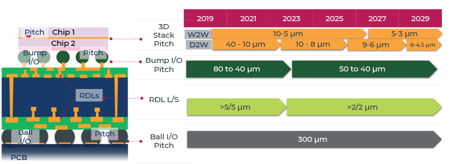
Source : Yole Développement
 July_GAI Topic|GAI trend reshapes the server industry chain
 August_Semiconductor|Advanced Packaging Technology for High Performance Computing Chips(M)