
矽光子專題|全球矽光子技術發展概況剖析(下)
In addition to silicon photonics process technology, interface technology is also a very important part of the process. Figure 2 shows the development of communication interfaces for data centers. The first copper cable connectors were used to route the telecom signals from the circuit boards to the switch chips. Copper cables were replaced by fiber optic cables, and then pluggable optical transceiver modules were used to convert the optical signals into telecom signals for transmission over the circuit board wiring to the switch chip. Twinax cables could be used to reduce signal degradation. In order to further reduce signal transmission loss, the development of On-Board Optics (OBO) technology, which installs optical transceiver modules on circuit boards to reduce the signal transmission distance, and the establishment of the COBO organization by Microsoft, Cisco, Broadcom, Arista, and other companies in 2015 in order to develop relevant standards. If optical signal transceiver modules can be fabricated into wafers using silicon photonics technology and integrated with the switch chip on the carrier board by means of co-packaged optical (CPO) technology, signal transmission loss can be significantly reduced, and with the increase in transmission capacity, the distance between the switch and the optical engine chip can be reduced to 50 μm as it evolves from a 2.5D package to a 3D package.
圖2、光通訊連接介面技術發展趨勢
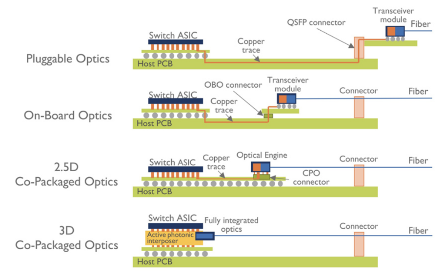
資料來源 : Yole Développement (2020)
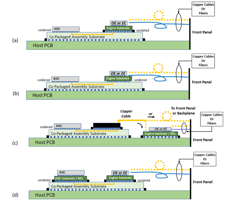
目前主要由交換器晶片設計大廠推動共封裝光學技術,研發此技術有Intel、Ayar Labs、Broadcom、Xilinx、Rockley、Cisco、Marvell、IBM、Nvidia、AMD、Juinper、日月光等公司,其中以Broadcom技術發展較快[為主要推動者],相繼於2022、2023年推出Tomahawk 4與Tomahawk 5等產品,2019年Microsoft、Meta等雲服務商成立聯盟以推動共封裝光學標準與產品。2022年Optical Internetworking Forum中展示目前發展出的四種共封裝光學架構,如圖3所示,
(a)與(b)是矽光子與交換器晶片封裝成多晶片模組(MCM),兩者的差異是矽光子晶片分別使用插槽連接或直接焊接在載板上。
(c)是交換器晶片和銅纜線組(Copper Cable Assembly)封裝成模組,再用纜線連接矽光子晶片。
(d)是矽光子與交換器晶片都是透過插槽連結載板,如此可方便安裝和拆卸晶片,這種架構稱為近封裝光學(Near-package Optics;NPO)。
圖3、目前發展出的四種共封裝光學架構
資料來源 : Optical Internetworking Forum (2022)
市場研究機構Yole Développement最新報告指出2022年全球共封裝光學市場規模為0.38億美元,預估至2033年將成長至26億美元,2022~2033年複合年增長率為69%。預估主要應用領域是資料中心、AI訓練/機器學習與分解式運算。檢視目前 400Gbps可插拔式光收發模組已經量產,且800Gbps產品也開始推出,
且由於共封裝光學產品尺寸小且更精密,若損壞時更換難度遠高於其他、尚未發展出統一規格,故當前仍無法與技術成熟、規格統一且成本低的可插拔式光收發模組技術競爭,換句話說可插拔式光收發模組在傳輸速度400Gbps或800 Gbps的產品主要採用之技術。預期1.6 Tbps以上光收發模組才會大量導入共封裝光學技術,市場研究機構Light Counting預估2027年可能成為市場主流。